
Modify the Linksys hardware

The described process for adding hardware to the Linksys WRT54GL router is a meticulous task that requires attention to detail and careful handling of components. The integration of UART connections via DB9 serial ports enhances the router's functionality, allowing for direct communication with the serial console and the Common Firmware Environment. This capability is essential for developers looking to run XINU on the device, as it provides the necessary interface to manage and interact with the firmware at a low level.
The selected components for the transceiver circuit, including the ADM202 chip, are specifically chosen for their compatibility with the 3.3-volt logic levels of the router. The conversion to RS-232 levels is crucial for standard serial communication, enabling the router to interface with a wide range of external devices and systems. The use of a custom PCB for the transceiver simplifies the assembly process, ensuring reliable connections and reducing the likelihood of errors during construction.
The assembly process involves several critical steps, including the careful soldering of headers and components, which must be performed with precision. The importance of verifying connections with a continuity tester cannot be overstated, as it ensures that the circuit is correctly established before applying power. This preventive measure helps to avoid potential damage to the router or the transceiver circuit due to incorrect wiring.
In summary, this comprehensive guide provides essential instructions for enhancing the capabilities of the Linksys WRT54GL router through the addition of UART connections and a transceiver circuit. The detailed descriptions of components, assembly techniques, and testing procedures are invaluable for anyone undertaking this project, ensuring a successful integration of hardware modifications.This will walk through adding hardware to a Linksys WRT54GL wireless router that will take advantage of existing connections on the PCB for two UART connections, which will be exposed as DB9 serial port connectors mounted to the faceplate of the router. These connections can be used to communicate with the serial console for XINU and also to inter act with the Common Firmware Environment `s command line interface. Gaining direct access to CFE is a key step towards being able to run XINU on the router. NOTE: The following lists all the necessary parts. However, the following tutorial describes assembling the transceiver on one of our custom transceiver boards. One could assemble the parts of the entire transceiver properly without the board, but with more difficulty.
Our transceiver board design is freely available for public use. Transceiver schematic is in postscript format, suitable for XCircuit. Transceiver PCB layout is in PCB format. Transceiver fabrication tarball contains Gerber photoplotter and CNC drill files suitable for professional fabrication. (No warranty express or implied, obviously. ) There are no screws or tools needed to open the router, just pop open the front with your thumbs as shown in the picture.
Some nice illustrated opening instructions can be found for a more detailed explanation of this step. First you need to unscrew the two screws keeping the router`s board attached to the case. Once the PCB has been removed from the case, locate the serial header holes provided by Linksys. This would be a grid of 10 holes (5x2) located on the bottom-right corner of the board when the antennae stubs are on top (see the top-down photo for clarification).
These ten holes hold all of the input and output for the two serial interfaces-UART0, and UART1-on the device. Now, we could just solder wires right onto these holes, but a by placing a nice 10-pin header on the board we can easily attach and detach a 10 connection cable.
Here you will use your soldering iron to solder the IDC shrouded double header onto the board. Make sure to note where the 1 pin is on the board (marked with a square around the hole instead of a circle) and where the 1 pin is located on the header (on ours it was marked with a triangle). Make sure that these two line up when soldering the header into the board. The next step is to build the transceiver circuit, which converts the 3. 3 volt serial signals from the router to conventional RS-232 serial voltages. The circuit includes only a handful of components, so it can be assembled using a small square of "perf board", or a variety of other inexpensive circuit prototyping techniques.
We use a custom-made printed circuit board to simplify assembly, as shown here. (Link to page with PCB specs, and directions. ) Again, you`ll need your soldering iron to secure the different pieces in the transceiver board. Using the diagram on the left, solder the shrouded double header, the socket, and the capacitors into the board in the appropriate places. NOTE: the positions of the components on the physical board are not represented in the diagram, but the silkscreen on the board indicates placement and orientation.
FURTHER NOTE: each component has a proper polarity or pin marking - direction matters! The pictures to the right show the transceiver board in various stages of completion. The top one shows the blank board on which the other components will be added. The bottom one shows the shrouded double header, the socket, and the capacitors soldered in place. It also shows the actual ADM202 chip inserted into the socket, however, before inserting the chip it is a good idea to test what you`ve completed so far. Use a continuity tester to check the connection between the header soldered into the router`s board and the socket on your transceiver board.
The next step we recommend for testing your work is to plug in the router and use a voltmeter to ch 🔗 External reference
Related Circuits
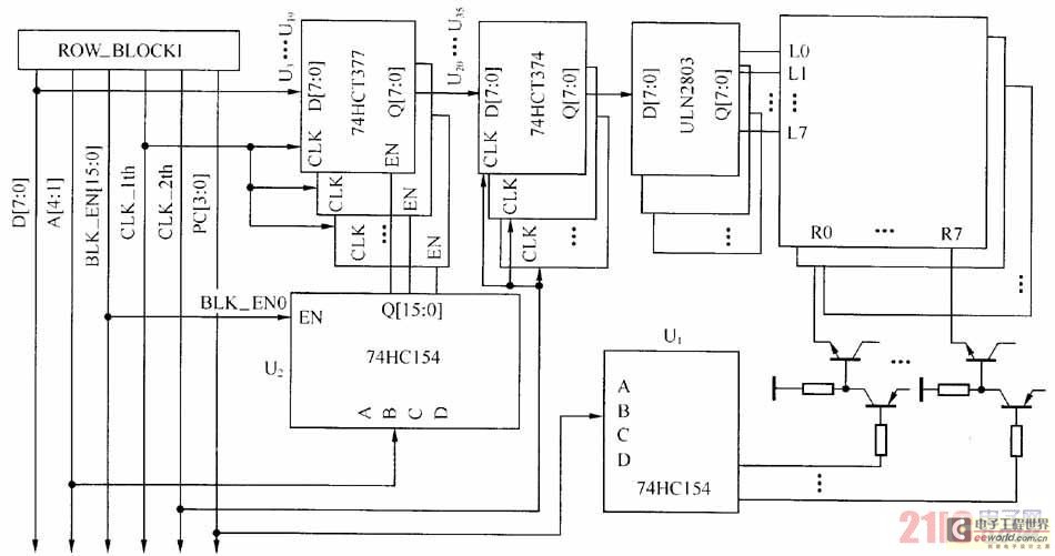
The large-scale LED display system utilizes a line-by-line scanning method and outlines the driving mechanisms to reduce hardware costs. It employs a 1/16 non-interlaced scanning mode, accommodating a total of 16 LED display panels. The schematic diagram of the...
The datapath consists of registers, an ALU, and an internal system bus. Registers are fast memory locations internal to the CPU, distinct from main system memory, and serve as temporary storage during calculations. The ALU is a combinational logic...
The Openbench Logic Sniffer is an open-source logic analyzer designed to support the SUMP logic analyzer software at minimal cost. Source and design files can be downloaded from the Gadget Factory project page. The project originated from discussions in...
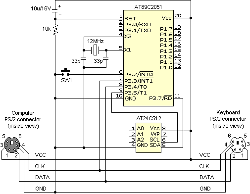
The Atmel AT89C2051 keylogger circuit connects to a PC keyboard via a PS/2 connection cable, facilitating data transfer between the keyboard and the circuit during program execution. The Atmel AT89C2051 microcontroller is a popular choice for implementing keylogger circuits due...
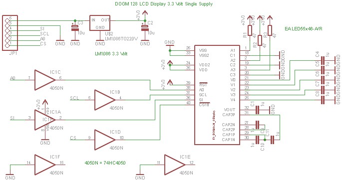
The DOGM graphics module should be connected to the Arduino board as illustrated. Pin 12 (MISO) of the Arduino board must remain unused. Furthermore, the DOGM graphics module requires an address line (A0), which can be connected to any...
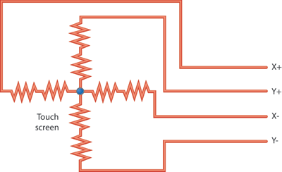
Touch screens are increasingly popular, yet many developers have never designed one. This guide provides a step-by-step approach to the necessary hardware and software for successful touch screen implementation. Touch screens are ubiquitous in industrial control systems, consumer electronics,...