
P8 CPU Documentatio Hardware

The P8 CPU's architecture is designed to optimize the interaction between its components, ensuring efficient processing of instructions. The registers play a crucial role in high-speed data handling, allowing for quick access and modification during computation. The ALU's design, utilizing two 4-bit units, enables the execution of a comprehensive range of arithmetic and logical operations, essential for the CPU's functionality. The careful arrangement of control signals ensures that the ALU operates correctly, responding to the current instruction's demands while maintaining synchronization with the internal bus and registers.
The conditional logic implemented through the Z register facilitates basic decision-making processes within the CPU, allowing it to branch based on the results of operations. This capability is fundamental for executing more complex algorithms and control structures within programs. The architecture's limitation of 256 bytes of addressable memory and 256 I/O ports reflects a design choice that balances complexity and cost, making the P8 CPU suitable for specific applications while highlighting the trade-offs inherent in hardware design.
Overall, the P8 CPU's architecture exemplifies a well-structured approach to CPU design, focusing on efficient data handling, robust operational capabilities, and a clear separation of functional components, all of which contribute to its effectiveness in executing a defined instruction set.The datapath contains registers, an ALU, and an internal system bus. Registers are very fast memory locations that are internal to the CPU and separate from the main system memory. They can be used as "scratch pads" during calculations. The ALU is a combinational logic device that performs arithmetic and logical operations on data. The internal bus p ermits data exchange between the ALU and registers. The control section interprets each instruction to be executed and asserts the datapath`s control signals in the proper sequence to implement the instruction. After executing an instruction, it proceeds to the next instruction. The following requirements and constraints were placed upon the hardware. In some cases they were contradictory, and a compromise was reached that favored reduced cost and/or construction time.
1. It must, of course, meet the specifications outlined in Section 2. 5 and implement the complete instruction set described in Section 3. 7. No compromise on this point is permissible. The programmer`s model defines the architecture of a computer. t is a high-level "machine" that is visible to the programmer, but independent of the actual physical hardware. It deals with the functional behavior of the computer as seen by the programmer. It includes the number and sizes of registers, types of instructions, addressing modes, and available memory.
See Section 3 for more information on many of the architectural features of the P8 CPU. The P8 CPU consists of three 8-bit registers and one 1-bit condition register. See Figure 4. 1. It is an accumulator-based design. This means that the number in the accumulator (A register) is an operand for most ALU operations. Additionally, all ALU results are placed in the A register, and overwrite its previous contents. It is also used for reading input ports and writing output ports. The R register may be used to store general data or a second operand. It also contains the memory address of operands for instructions using indirect addressing. Because the instruction pointer is an 8-bit register, only 256 bytes of memory may be addressed. Similarly, there are 256 available I/O ports, which do not share the memory space. The Z register is a 1-bit register that stores the results of the last compare operation. If the result was zero, the Z register contains a "1", otherwise it is "0". One 8-bit ALU is needed to implement the arithmetic and logical instructions. Actually, the decision of which ALU instructions to include in the instruction set was dictated by the only TTL ALU available - the 74181. Because this is a 4-bit ALU, two of them are required. See Figure 4. 4. This ALU can generate condition bits for carry, half-carry, A=B (or zero), A>B, and A
) The "CN+4" output of the least significant 4-bit ALU must be connected to the "CN" input of the most significant 4-bit ALU to create an 8-bit ALU. This connection allows a carry between bit 3 (MSB of first ALU) and bit 4 (LSB of second ALU) and generates the correct 8-bit result during an ALU operation.
"CN" of the least significant ALU must be low for a subtract operation and high for all others. This input, as well as the select and mode inputs, are asserted by the control logic of the CPU. The control logic properly configures all inputs for the desired ALU operation. The control logic accepts inputs from IR and the ALU (through Z) and generates as output all the control signals necessary for the correct operation of the datapath. There are two approaches that can b 🔗 External reference
Related Circuits
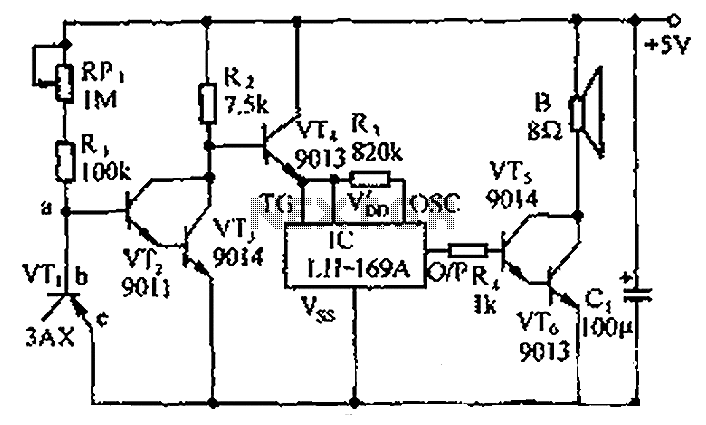
The circuit consists of a temperature sensor, electronic switches for temperature control, and a vocal language output system. During hot summer months, the central processing unit (CPU) of PCs frequently experiences overheating. The circuit, with VT1 positioned near the...
A lens is a customized view of content within a repository, allowing users to perceive information through the perspectives of trusted organizations and individuals. In electronic systems, the concept of a "lens" can be metaphorically related to circuit design methodologies...
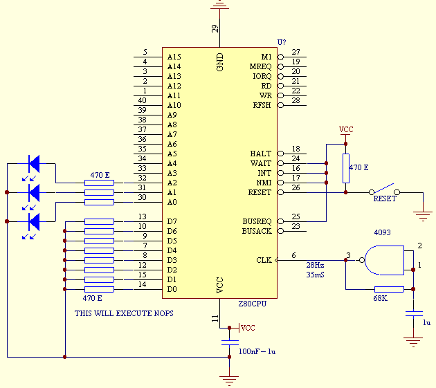
GND and VCC are positioned perpendicularly to the other pins in the circuit diagrams, while the actual Z80 is a DIP with no pins in these locations. This arrangement complicates the readability of the circuit diagram, necessitating a mapping...
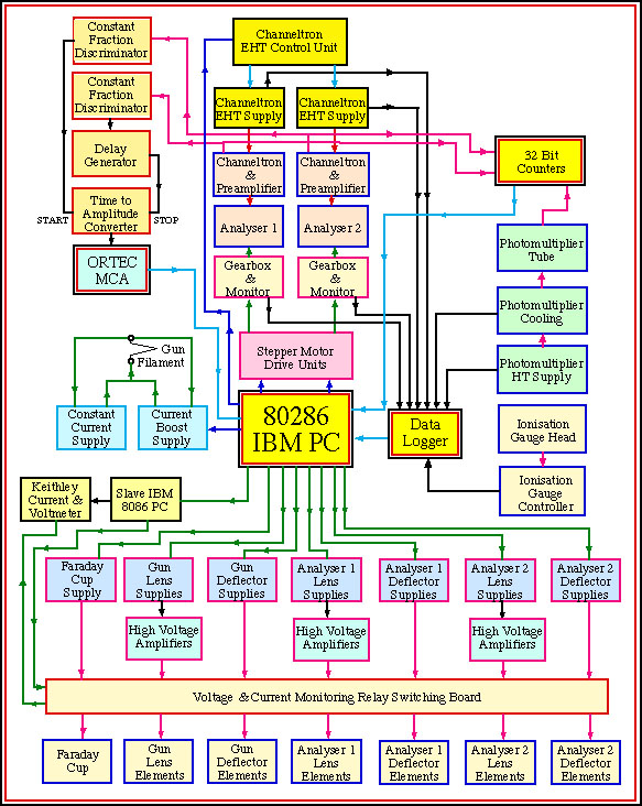
The spectrometer vacuum chamber is constructed from 304-grade stainless steel, with the design executed by Vacuum Generators based on the work of Jones, Read, and Cvejanovic, detailed in T. Jones' Ph.D. thesis from the University of Manchester (1984). The...
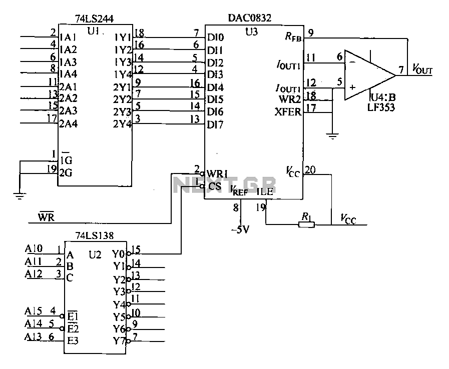
The DAC0832 is depicted in Figure 27-13 as a single-phase circuit connected to the 8086 CPU. The internal 8-bit data input of the DAC0832 must be interfaced with the CPU and the D/A converter interface circuits for data transmission,...
When the water level is low, the wires in the tank are open-circuited, and the 180K resistor pulls the switch low, resulting in the switch opening and the LEDs turning OFF. As the water begins to fill the tank,...