
monostable multivibrator 555 timer

The 555 Timer in monostable mode is a versatile component widely used in various applications such as timers, pulse generation, and frequency modulation. The circuit typically consists of the 555 Timer IC, a resistor (R), and a capacitor (C) that determine the time period for which the output remains high after being triggered. The resistor and capacitor values can be selected based on the desired timing requirements, allowing for a wide range of pulse widths.
The operation begins with the application of a negative pulse to the Trigger pin, which momentarily sets the output high. This transition triggers the internal flip-flop of the 555 Timer, which controls the output state. The charging of the capacitor through the resistor R causes the voltage across the capacitor to rise gradually. The time taken for the capacitor voltage to reach 2/3 Vcc can be calculated using the formula T = 1.1RC, where R is the resistance in ohms and C is the capacitance in farads.
The Reset pin is critical in ensuring that the circuit does not inadvertently reset during operation, which could disrupt the timing sequence. Grounding the Control Voltage pin with a capacitor serves to stabilize the internal reference voltage, minimizing the effects of noise that could affect the comparators' performance.
In summary, the monostable mode of the 555 Timer is a reliable and efficient method for generating precise timing pulses, with the output state being controlled by external components and the internal logic of the timer. The design allows for easy adjustments of the timing parameters, making it suitable for a variety of electronic applications.As its name indicates it has one stable state and it switches to unstable state for a predetermined time period T when it istriggered. The time period T is determined by the RC time constant in the circuit. Monostable mode of 555 Timer is commonly used for generating Pulse Width Modulated ( PWM ) waves. This is the circuit diagram of 555 Timer wired in Monostable mode. 8th pin and 1st pin of the 555 timer are used to givenpowerVcc and Ground respectively. 4th pin is the Reset pin of 555 Timer, which is active low so it is connected to Vcc to avoid accidental resets. 5th pin is the Control Voltage pin used to provide external reference voltage to internal comparators.
Since it is not used here, it is grounded via a capacitor C` (0. 01 µF) to avoid high frequency noises. When a negative trigger is applied on the Trigger input of 555, output goes high and capacitor starts charging through resistor R. When the capacitor voltage becomes greater than 2/3 Vcc, ouput goes low and capacitor starts discharging through the Discharge pin of 555 Timer.
Time period of the unstable state is given the tye expression, T = 1. 1RC. When a negative trigger is applied to the Trigger pin of 555 Timer, output of lower comparator will become HIGH and output of upper comparator will be LOW, since the capacitor voltage is zero. This makes the output HIGH. After the negative trigger, output of lower comparator becomes LOW and that of upper comparator remains LOW.
Since both inputs of the SR Flip Flop are LOW, output will not change, so the output is HIGH. When the capacitor voltage will become greater than 2/3 Vcc, output of upper comparator becomes HIGH and that of lower comparator remains LOW, so the output becomes LOW. 🔗 External reference
Related Circuits
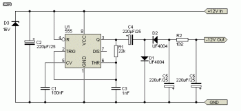
This is a voltage doubling circuit built using the well-known timer IC 555. The circuit is straightforward and easy to construct. The construction is not critical. Rectifier diodes should be ultrafast (such as UF4004 or similar), or 1N4148 signal...
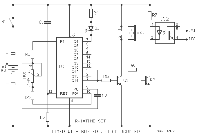
A small circuit that can find a lot of applications for measuring time. It has the capability to inform with a sound signal from the BZ1. At the same time, there exists the possibility to drive an external circuit...
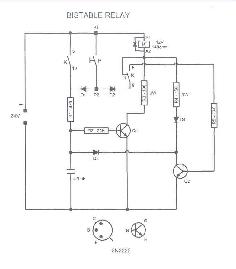
This circuit could be used to drive a monostable relay by a single momentary switch. Powered by 24 Volts, it works for a 12 Volts relay. When the button is pressed, Q1 is energized and the capacitor charges, while...
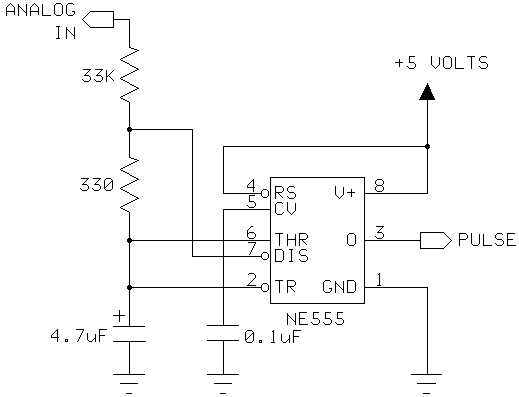
I had a Basic Stamp project that needed to measure a nominal 12 volt battery, and I wanted a simple solution. This is the simplest I could come up with. The 555 timer will put out positive pulses. The...
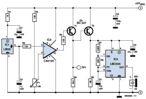
The overhead detector (fire alarm) circuit utilizes a precision integrated temperature sensor, the LM35 (IC1), which offers an accurate linear output. The overhead detector circuit is designed to monitor ambient temperature levels for fire detection purposes. The core component of...
When this circuit is activated, the inherent offset of the devices acts as an automatic starting voltage. The output voltage V0 becomes positive, and the positive feedback through R2 and R1 drives the output to saturation. The elevated voltage...