
Morse Keyer Redesign and Rebuild
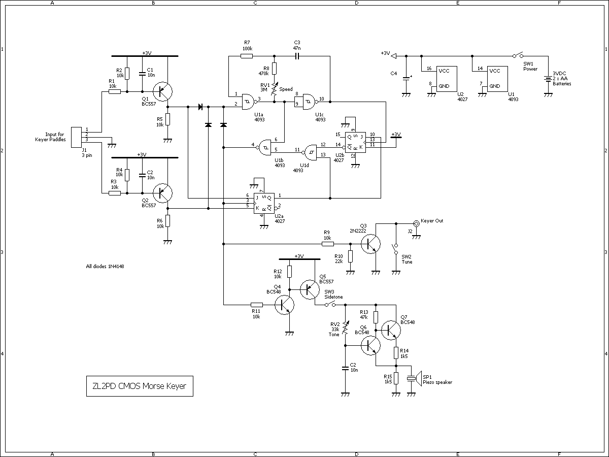
The transformation of the traditional TTL-based Morse keyer into a modern CMOS version involves several key considerations in circuit design. The primary components include two CMOS ICs, which serve as the core logic elements, replacing the outdated TTL chips. The use of CMOS technology not only reduces power consumption significantly but also enhances the overall reliability of the keyer.
The schematic for the iambic Morse keyer would typically include the following sections:
1. **Power Supply Circuit**: A low-dropout voltage regulator can be employed to ensure a stable 5V output from a battery source. This minimizes the power loss and heat generation, making it suitable for battery operation.
2. **Microcontroller/CMOS Logic ICs**: The heart of the keyer, responsible for processing the paddle inputs and generating the appropriate Morse code output. This section may include a simple microcontroller or a combination of CMOS logic gates configured to handle the input signals from the paddles.
3. **Input Paddle Interface**: This section consists of two paddles connected to the input of the CMOS logic. The circuit design should ensure that pressing either paddle generates a clean signal, which can be interpreted by the logic ICs without bounce or noise.
4. **Output Stage**: The output stage typically consists of a transistor driver that amplifies the signal to drive the keying circuit of a transmitter or oscillator. This stage may also include additional filtering to ensure that the output signal is free from distortion.
5. **Optional Memory Circuit**: For those interested in adding memory functions, a small EEPROM or RAM chip can be integrated into the design. This allows for the storage of common messages, enhancing the functionality of the keyer.
6. **User Interface**: Simple LED indicators can be included to provide feedback on the status of the keyer, such as power on/off and keying activity.
Overall, the transformation of the keyer from TTL to CMOS not only revitalizes the device but also aligns it with modern electronic standards, providing a lightweight, efficient, and user-friendly Morse code transmission solution.Two cheap CMOS ICs and a few transistors was all that was required to rebuild my elderly TTL automatic morse keyer into a low current lightweight battery powered iambic morse keyer. Sometime over the past year or two, my elderly Accu-Keyer gave up the ghost and died. I built it more than 30 years ago (!) from the original TTL IC-based design published in the ARRL Handbook. It was an accurate copy of the original, right down to the printed circuit board which I made using nail polish as resist and ferric chloride etchant. As I was tearing the old keyer apart, I instantly recognised the PCB production method I`d used by the quality of the resulting PCB.
It was not very pretty, and I certainly could not reuse the PCB simply by replacing the dead ICs with new CMOS devices. In those days, the Accu-Keyer was the most popular design. Most of those keyers used TTL chips, and the current drain worked out to be a few hundred milliamps. Running it off batteries was hardly practical, and I never tried. But there were times when it would have been useful. In fact, I was never very happy with the keyer. The power supply was my biggest gripe, and my own fault. I made it using a rewound transformer. I was a poor high school student in those days, without much money to spend on the hobby. To get the right voltage for the power supply - I needed 5VDC - I found a transformer somewhere, pulled it apart, and rewound the secondary by hand.
The problem was that the darned transformer used to hum like crazy because I was unable to clamp up the laminations adequately. I guess I could have dipped it in varnish or something, but I never got around to it. The hum wasn`t too bad when it was all enclosed inside the little box. Even so, every time I turned it on, I would hear that hum, and I`d mutter to myself about doing something about the transformer `one of these days`.
But while the keyer was working and usable, I just couldn`t be bothered. There were too many other things of more interest to build. A few months ago, however, I went to use the keyer again (You can tell how much CW I do!) only to find the keyer had died. I checked out a number of the chips, fixing my old TTL logic probe in the process (The first dry joint in 20+ years), only to find that almost all of the seven chips used in the old design had up and died.
I was prepared to replace one or two, but the widespread deaths of ICs across the PCB made me forget that idea. Keyers, or "Elbugs" as the Europeans call them, are used to send Morse code. Most keyers use a two-paddle key for operator inputs. Pressing either paddle towards the opposite paddle results in the keyer sending a series of either `dits` or `dahs`, depending on which paddle is pressed.
Unlike typical manual morse keys, keyers are designed to send near-perfect code, with `dahs` equal in length to three `dits`, and with precise inter-symbol timing. The really neat thing about the more advanced versions of these keyers, called `iambic` keyers, is that these allow you to insert a `dit` in a stream of `dahs`, or vice-versa, or send a string of `dit-dah` or `dah-dit` characters.
To send an `a` (`dit-dah`) merely requires a single squeeze of the paddles. Sending a `c` (`dah-dit-dah-dit`) take no more effort - A single, slightly longer, squeeze does the trick. The objective of these keyers is to reduce the effort of sending Morse code manually. While computerized keyboard keyers also exist, they are not as portable as these keyers, and certainly nowhere near as popular.
Modern keyers are almost all microprocessor-based, and include memories to hold standard messages. These provide storage for `CQ` calling messages, and routine sentences which regularly occur during a call such as the operator`s name, location and equipment details. Most also add specialized auto-numbering messages for use in contests. Some older TTL or CMOS designs also supported memories, but these desi 🔗 External reference
Related Circuits
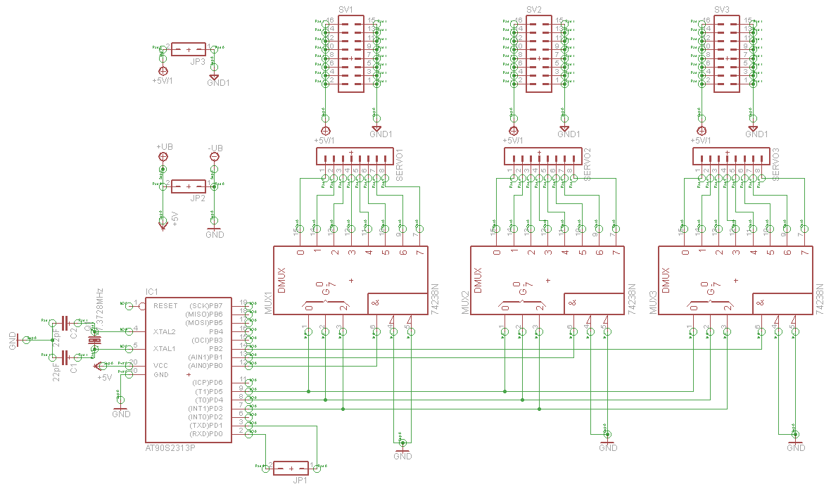
A serial servo controller is being developed to enhance knowledge of electronics and assembly language as part of a hexapod robot project. Initially, the ATTiny2313 microcontroller was utilized; however, it became evident that additional I/O channels were necessary. Consequently,...
This video demonstrates how to initiate multiple instances of QsoNet's Dahdidah CW Software Keyer using FABULATECH's Virtual Serial Port Splitter. Four separate... The QsoNet Dahdidah CW Software Keyer is a sophisticated tool designed for amateur radio operators, allowing them to...
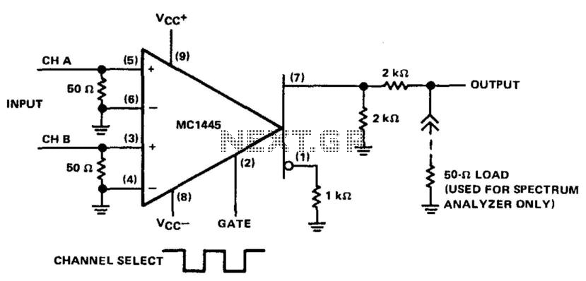
Apply a signal to each differential amplifier input pair. When the gate voltage changes from one extreme to the other, the output can alternate between the two input signals. When the gate level is high (1.5 V), a signal...
The vacuum tube remains relevant and functional in certain applications, such as in this continuous wave (CW) transmitter. The circuit is constructed in a traditional breadboard style on a wooden base. Old table radios serve as a valuable source...
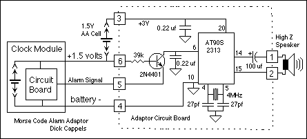
Almost trivial application of an AT90S2313 or ATtiny2313 in an alarm clock to change the alarm from "BEEP BEEP BEEP BEEP BEEP BEEP BEEP BEEP..." to "WAKE UP" in Morse code. This was designed in response to a request...

This is an improved version of the audio interface commonly used to connect a computer soundcard to a transceiver's receive and transmit audio circuits. This kind of interface is used by computer programs that send and receive SSTV, RTTY,...