
MOSFET FM Transmitter Circuit

The MOSFET FM transmitter circuit operates by utilizing several key components that work in concert to produce a stable and clean FM signal suitable for aligning FM radio receivers. The circuit begins with a microphone amplifier that captures audio input. This amplifier is equipped with automatic gain control (AGC) to maintain a consistent audio level, preventing distortion from overly loud inputs.
The heart of the modulation process is a voltage oscillator, which generates a carrier frequency. This oscillator, represented by T2 in the schematic, is crucial for frequency modulation. The modulation is accomplished through the use of a double diode configuration (D4/D5), which alters the capacitance in response to the audio signal, effectively modulating the carrier frequency.
The output from the oscillator is a frequency-modulated signal that appears at the drain terminal of T2. This signal is then passed to another MOSFET, T3, which serves as an amplifier, boosting the signal strength before transmission. To ensure that the output signal is free from unwanted high-frequency noise, a low-pass filter is integrated into the circuit. This filter allows only the desired frequency range to pass through, providing a clean FM signal for transmission.
The output power is adjustable, ranging from 10 to 50 mW, allowing for flexibility depending on the application requirements. The amplitude of the amplified audio signal can be fine-tuned using potentiometer P1, enabling the user to optimize the audio quality before transmission.
Finally, the clean FM signal is fed to an antenna, where it can be broadcasted to FM radio receivers. This circuit design is particularly useful for hobbyists and professionals looking to create a reliable FM transmitter for various applications, including educational projects and personal use.This mosfet fm transmitter circuit is designed to be used for aligning FM radio receivers. It has a microphone amplifier with automatic gain control. The FM modulation is a voltage oscillator and the final stage is built with MOSFETs. A lowpass filter at the output assures the transmission of a clean 10 50 mW FM signal. IC1 works as an amplifi er supplying a negative control voltage to FET T1. The amplitude of the amplified audio signal can be adjusted through P1. The carrier frequency is generated by the oscillator T2. The oscillation is frequency modulated through the internal capacitance changes of the double diode D4/D5. The frequency modulated appears at the drain terminal of T2. This signal is then amplified by T3 and passes through the lowpass filter before finally arriving at the antenna.
🔗 External reference
Related Circuits
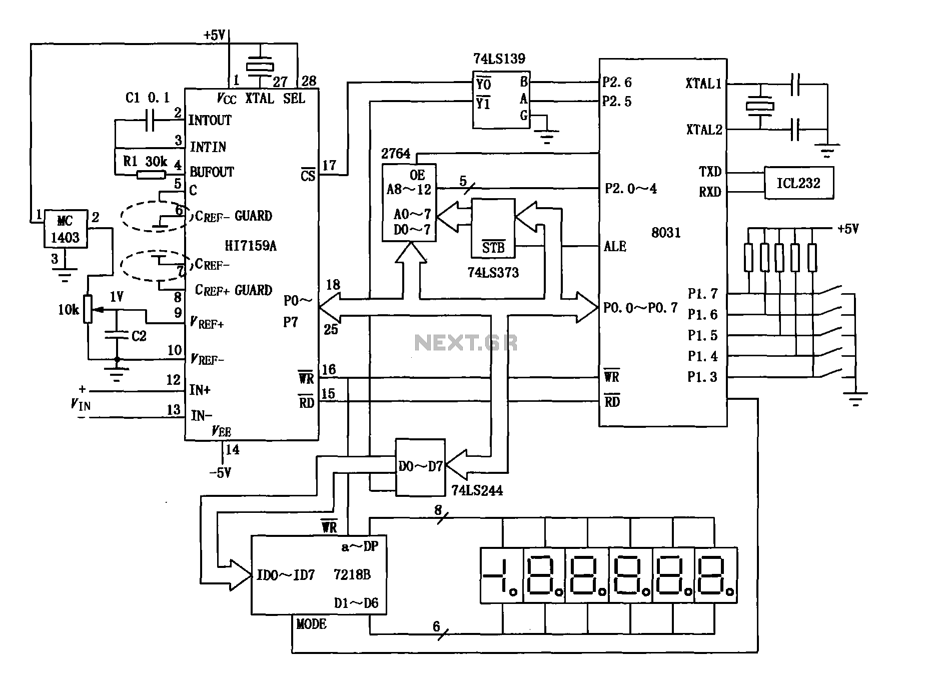
An intelligent digital voltmeter circuit utilizing the HI7159A, 8031 microcontroller, and various other components as illustrated in the figure. The internal circuit incorporates a successive cumulative integrator, digital zero function, low noise BIMOS technology, and other advanced features. In...
By utilizing logic chips, the behavior of a robot can be enhanced, allowing for the implementation of more complex algorithms. Logic chips, also known as logic gates or digital logic integrated circuits, are fundamental components in digital electronics that perform...
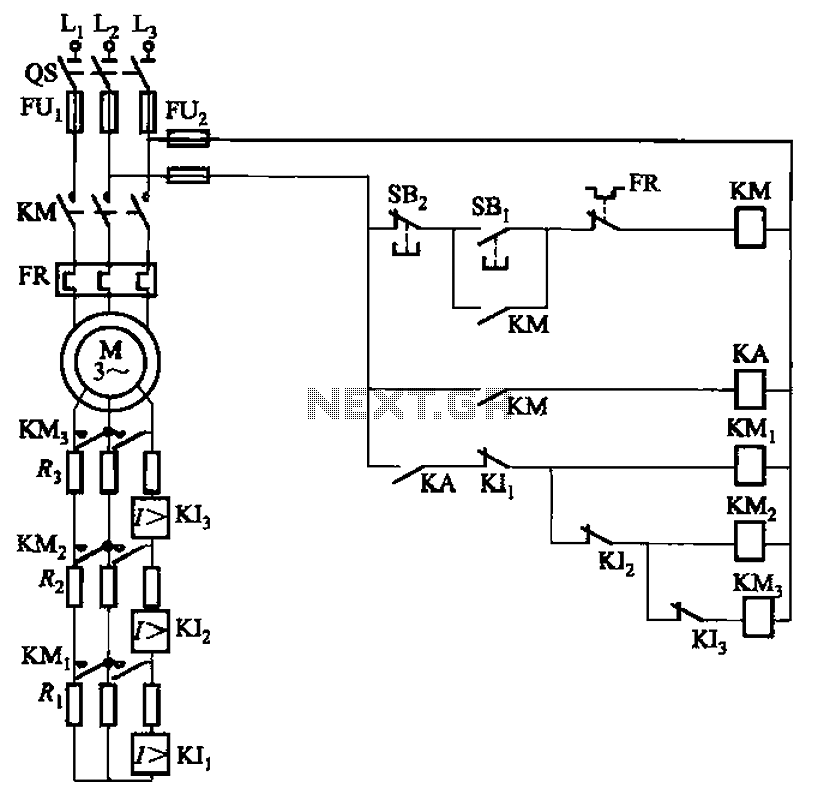
The circuit illustrated in Figure 3-161 features a first stage current detection mechanism utilizing a current relay (KI1) in series with a resistor (R1). The second stage employs another current relay (KI2) in series with a resistor (R2) for...

This is an application circuit for calibration known as a high voltage AC calibrator circuit. A key aspect of sine wave oscillator design is the stable control of amplitude. In this circuit, the amplitude is stabilized through servo control,...
The ZN414 integrated circuit (IC) contains a complete automatic gain controlled AM receiver within a compact three-pin package. With only a few external components, it is possible to construct a simple radio that offers excellent selection and reception capabilities....
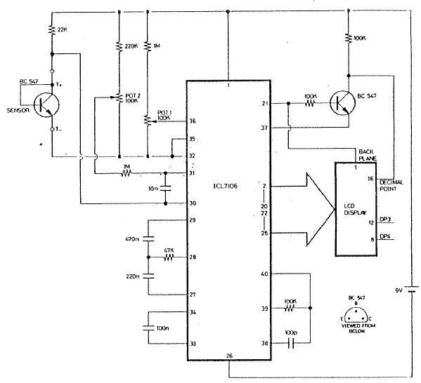
The ICL7106 integrated circuit contains all the active circuitry for a 3 1/2 digit panel meter (DPM) in a single chip. It was designed to interface directly with a liquid crystal display (LCD). The potential difference across a silicon...