
mosfet low dropout charger circuit

The low dropout charger circuit primarily aims to maintain battery charging efficiency while minimizing the voltage drop across the pass element, which in this case is a MOSFET. The use of a MOSFET allows for better thermal performance and efficiency compared to traditional linear regulators.
In this design, Q2 serves as the primary pass element, handling the majority of the charging current. It is essential that Q2 is rated for at least 0.2 A to ensure reliable operation under load conditions. The selection of a suitable MOSFET with low on-resistance will further enhance the efficiency of the charging process.
Q3, being a low current device rated at 2 A, functions to provide additional control over the charging process. Its role is critical in conjunction with the Schottky diode, which is used for its low forward voltage drop and fast switching characteristics. This diode prevents backflow of current from the battery to the charger when the input voltage is absent, thereby protecting the circuit and preserving battery charge.
The circuit's simplicity is one of its key advantages, making it suitable for various applications where space and cost are constraints. However, it is important to note that the absence of current limiting can pose a risk of overcurrent conditions, which could lead to potential damage to the battery or the circuit components. Therefore, in applications where current management is critical, additional circuitry may be required to implement current limiting features.
Overall, this low dropout charger circuit represents a practical solution for battery charging applications, provided that the limitations regarding current management are acknowledged and addressed as necessary.This circuit is design circuit for low drop out charger using a MOSFET as the pass element, but this circuit does not include current limiting. This is the figure of the circuit. This circuit is a simple design. This circuit uses Q3 and a Schottky diode to isolate the battery from the charging circuitry when the input voltage is removed, to preven
t the battery from discharging. Q2 should be a high current (0. 2 ©) FET, while Q3 can be a low current (2 ©) device. 🔗 External reference
Related Circuits
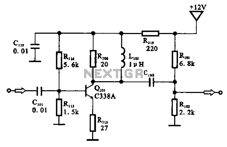
The amplifier circuit is designed as a pre-amplifier configuration. It utilizes transistor Q101 and other components such as inductor L101 and biasing elements. The transistor operates as a common emitter intermediate frequency (IF) amplifier. The IF signal is coupled...
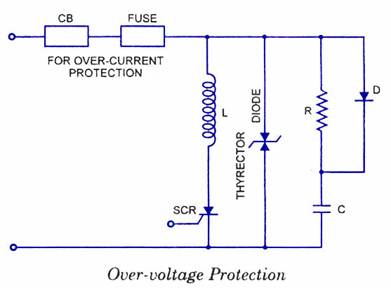
Silicon Controlled Rectifiers (SCRs) are sensitive to high voltage, over-current, and transients. To ensure satisfactory and reliable operation, they must be protected against such abnormal operating conditions. Due to the complexity and cost of protection mechanisms, devices with ratings...
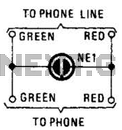
A neon lamp can easily be added to the phone line to act as a ring indicator. It is perfect for times when you cannot hear the phone. The integration of a neon lamp as a ring indicator in a...
The Zener diode may not be providing sufficient current in its breakdown state to activate the transistor. Removing resistor R2 did not resolve the issue. The Zener's voltage selection could be too high, potentially preventing it from regulating the...
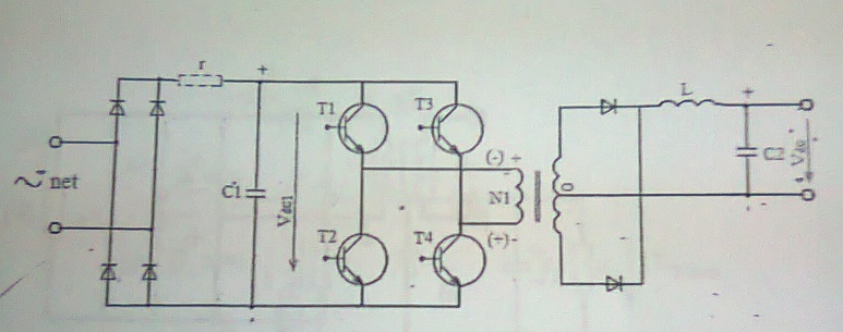
A power supply with frequent energy switching; however, the schematic is incomplete. An additional circuit is needed to control the voltage polarity converter, which consists of four transistors. This circuit generates high-frequency current pulses. Assistance is appreciated to explain...
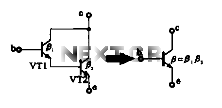
There are two composite pipe configurations: one consists of two transistors of the same type, while the other is made up of two different types of pipe configurations. The first configuration, utilizing two transistors of the same type, typically involves...