
Multifunction appliance protection circuit diagram
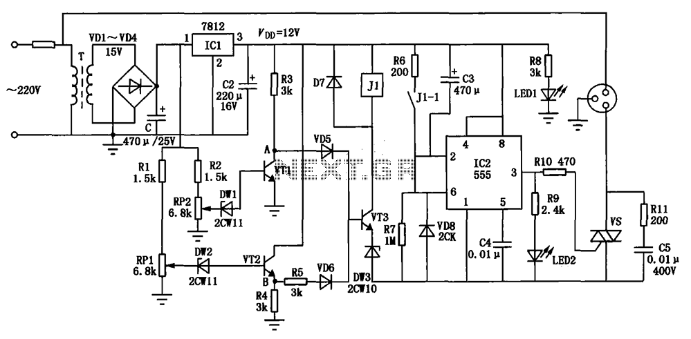
The described circuit is a comprehensive DC voltage regulation and protection system designed to maintain a stable output voltage while safeguarding against potential electrical faults. The primary component, the LM7812 voltage regulator, is responsible for providing a consistent 12V output, making it suitable for various electronic applications that require a reliable power supply.
The undervoltage and overvoltage protection mechanisms are critical to ensure the circuit's longevity and reliability. These protections are achieved through a combination of resistors (R2 and RP2) and regulators (DW1 and DW2), which monitor the input voltage levels. If the voltage falls below or exceeds predefined thresholds, the circuit activates protective measures to prevent damage to connected components.
Transistors VT1 through VT3 are utilized within the circuit to facilitate switching operations. The choice of the 3DG4 transistors allows for efficient control of the relay (J1), which is used to disconnect the load in case of an overvoltage or undervoltage condition. The relay, specified as JRC-1M 12V, is designed to handle the switching requirements of the circuit effectively.
The OR circuit, which includes diodes VD5 and VD6, plays a crucial role in ensuring that the protection mechanisms can operate simultaneously without interference. This arrangement allows for a robust response to voltage fluctuations, enhancing the overall reliability of the circuit.
Diodes VD1 to VD7, selected as 1N4004, provide additional rectification and protection against reverse voltage conditions, further stabilizing the output and ensuring that the circuit operates within safe parameters. The thyristor VS, rated at 6A/400V, adds to the circuit's ability to manage high current loads while maintaining safety and performance.
Overall, this DC voltage regulator circuit, complete with delay and protection features, is engineered to deliver a stable and secure power supply, making it suitable for a wide range of electronic applications where voltage regulation and fault protection are essential. Circuit is shown, which consists of a DC voltage regulator circuit, the delay circuit, overvoltage and undervoltage protection part of the implementation of circuit, and the li ke. ICl integrated voltage regulator circuit LM7812 + 12V output voltage. Undervoltage and overvoltage protection circuit sampling by the R2, potentiometer RP2, the regulator DWl, VTl and Rl, RPl, DW2, VT2 and OR circuit VD5, VD6, VT3, control relays J1 constitution.Figure, VT1 ~ VT3 selection 3DG4, thyristor VS selection 6A/400V, VD1 ~ VD7 selection 1N4004, relay J1 selection JRC-1M 12V.
Related Circuits
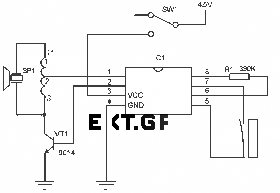
The alarm circuit operates as follows: When the power switch SW1 is turned on, the alarm system becomes active. If a magnet is brought close to the spring, the magnetic field attracts the spring, causing the dynamic and static...
This document discusses the creation of an electronic spy bug circuit using two methods: one involving a wired connection from the transmitter to the receiver, and the other being a completely wireless setup capable of eavesdropping on conversations up...
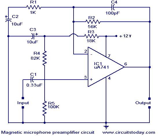
A preamplifier for magnetic pickups of record players is presented. The uA 741 is utilized as an AC-coupled non-inverting amplifier operating on a single supply. The amplifier gain is determined by the feedback components, where C2 manages the low-frequency...
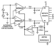
The Common Mode Rejection Ratio (CMRR) facilitates the rejection of high-frequency common-mode voltages, leading to the attenuation of elevated ambient noise levels from utility lines, industrial machinery, and other sources of radiation. The circuit diagram presented illustrates the advantages...
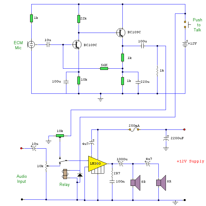
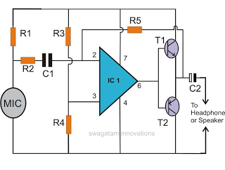
This circuit prioritizes a microphone and preamplifier (voice circuit) over any other audio signal, functioning similarly to a one-way intercom. When the push-to-talk switch is activated, the main amplifier switches from music to the voice signal. Essentially, a voice-over...
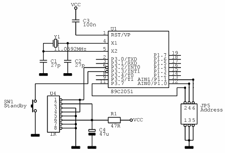
The circuit utilizes an infrared (IR) receiver chip to capture IR signals from a remote control. This chip features a bandpass filter and a demodulator, resulting in a logic-level output. The controller section is based on a standard 8051...
Warning: include(partials/cookie-banner.php): Failed to open stream: Permission denied in /var/www/html/nextgr/view-circuit.php on line 713
Warning: include(): Failed opening 'partials/cookie-banner.php' for inclusion (include_path='.:/usr/share/php') in /var/www/html/nextgr/view-circuit.php on line 713