
Remote Control Circuit
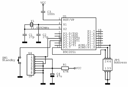
The circuit design incorporates an IR receiver chip that effectively demodulates incoming IR signals, providing a reliable logic signal output for further processing. The 8051-based controller is a compact and efficient microcontroller that manages the overall operation of the circuit. The necessity for programming the AT89C2051 chip emphasizes the importance of firmware development, which dictates the functionality of the device.
The power management features are significant, as the inclusion of interrupt inputs allows the microcontroller to conserve energy by remaining in a sleep state until an external event, such as a signal from the IR receiver or the activation of the power switch, occurs. This is particularly beneficial in battery-powered applications where energy efficiency is critical.
The address jumper (JP5) facilitates the selection of specific communication addresses in accordance with the RC5 protocol, which is widely used in remote control applications. Proper configuration of this jumper ensures compatibility with various remote controls that utilize the same protocol.
The output stage of the circuit is designed to control motors or other loads in two directions, utilizing a complementary transistor arrangement. The careful design of the control logic prevents both Q1 and Q2 from being turned off simultaneously, which could lead to potential damage or erratic operation. The implementation of separate output transistors (Q3, Q4, Q5, and Q6) for each direction enhances the reliability and functionality of the circuit, ensuring smooth operation during volume adjustments or other controlled movements.
Overall, this circuit exemplifies an efficient design for IR remote control applications, integrating power management, programmable logic, and effective output control in a compact configuration.The circuit uses an IR receiver chip to receive the IR signal from the remote. The chip includes a bandpass filter and a demodulator, so the output is a logic signal. The controller section is more or less a standard 8051 circuit - the controller chip is basically an updated Intel 87C51 with less pins. Please note that the controller chip has to b e programmed. If you buy an AT89C2051 chip it`s "empty", so the circuit won`t do anything. The "power off" switch SW1 as well as the output from the IR receiver are connected to the chip`s two interrupt inputs. That means the chip can be "put to sleep" most of the time, because signals on those two pins can wake it up.
The address jumper JP5 is used for selecting the RC5 address. Read more in the "Protocol" section. The header JP6 is used for setting options like B+ delay. When the volume pot has to be moved, the base of either Q1 or Q2 is driven low switching off the transistor. This enables two of the output transistors to switch on. Q3 and Q5 switch on for one direction and Q4 and Q6 for the other direction. If both Q1 and Q2 are switched off at the same time strange things may happen. So that mode of operation is not supported by the standard software ;-) 🔗 External reference
Related Circuits
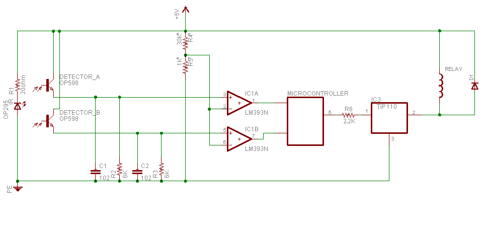
Sensing unit consists of infrared emitter OP295 to produce the infrared beam, and two detectors in front of the emitter to detect the infrared beam OP598. Since the main idea in this device is to know person direction; and...
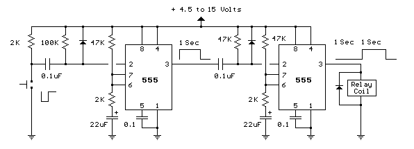
This toggle circuit utilizes two 555 timers configured as inverters. Pins 2 and 6 serve as the threshold and trigger inputs for the first timer, while pin 5 provides the output. The output at pin 5 will consistently reflect...
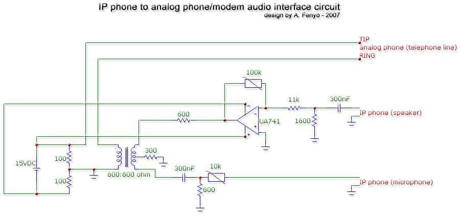
The transformer is a 600:600 ohm transformer, also referred to as a 1:1 ratio 600 ohm transformer. It has approximately the same number of turns on both the primary and secondary coils and is optimized for operation at a...
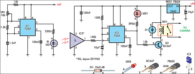
This circuit serves as an alternative to the infrared (IR) beam break detector featured in the June 2009 issue of Silicon Chip. To enhance its insensitivity to ambient light, it employs a standard IR receiver integrated circuit (IC), such...
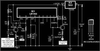
This is a circuit diagram for automatic muting in audio systems utilizing the IC LB1403. The output from a pre-amplifier, such as the LA3160, LA3161, or HA1032, is connected to the base of the amplifier transistor BC548 (T1). A...

A gyrator is a circuit that utilizes active devices and transistors to emulate an inductor. In this instance, the gyrator comprises a transistor in conjunction with resistors R1, R3, and capacitor C2. Alternatively, a unity gain operational amplifier could...