
Multiplexed bcd-to-parallel bcd converter
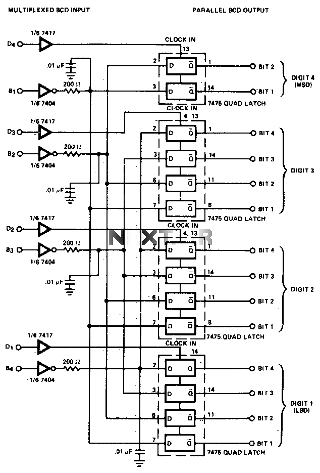
The converter utilizes four quad bistable latches, each capable of storing a single bit of information. These latches are arranged in a manner that allows them to be triggered sequentially by the digit strobe output from the LD110, which serves as a timing reference for the operation. When the digit strobe signal transitions from low to high, it activates the latches, causing them to capture and reflect the current state of the bit outputs. This operation is crucial for applications requiring precise timing and data integrity.
The complemented outputs (Q) provide an inverted representation of the stored data, enabling easy interfacing with other digital components that may require active-low signals. Once the digit strobe signal goes low, the latches maintain their last captured state, ensuring that the data remains stable and unaffected by further changes in the strobe signal. This feature is particularly important in digital systems where data consistency must be preserved during processing cycles.
In terms of circuit design, the layout would typically include power supply connections, ground, and appropriate signal routing to ensure that the strobe signal reaches all latches simultaneously. Additional components such as pull-up or pull-down resistors may be incorporated to enhance signal integrity and prevent floating states during transitions. The overall design should also consider the propagation delay of the latches to ensure that the timing of the digit strobe signal aligns with the desired operation of the system.Converter consists of four quad bistable latches activated in the proper sequence by the digit strobe output of the LD110. The complemented outputs (Q) of the quad latch set reflects the state of the bit outputs when the digit strobe goes high.
It will maintain this state when the digit strobe goes low. 🔗 External reference
Related Circuits
A voltage-to-frequency converter with a control range of 1:1000 can be constructed using the IC TSC9402. The specified component values in the circuit yield a conversion factor of 1 kHz per 1 V. Input voltages ranging from 10 mV...
In the NIXIE clocks constructed, a large mains transformer was avoided within the clock itself by using an AC adapter that connects to the mains wall plug. This necessitated the use of an up-converter to generate the 180V anode...
Build an interface board to connect scientific equipment, specifically a pair of photovoltaic tubes, to a personal computer for acquiring measurement results. The signal properties include two channels with a common ground, a one-second acquisition time, and a maximum...
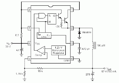
Switching regulator subsystems intended for use as DC to DC converters. 3V to 40 Volt DC Converter circuit. The use of switching regulators is becoming more pronounced than that of linear regulators because the size reductions in new equipment...
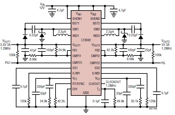
A 3.3V and 5V DC-DC converter circuit design project utilizing the LT3692 dual tracking regulator. The LT3692 is a highly efficient dual-output DC-DC converter designed for applications requiring both 3.3V and 5V outputs. This integrated circuit can provide a regulated...
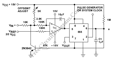
This is a circuit for a Voltage-to-Pulse Duration Converter. The circuit is designed to convert voltage into pulse duration by integrating a timer IC and an operational amplifier (OP Amp). The Voltage-to-Pulse Duration Converter circuit utilizes a timer IC, typically...