
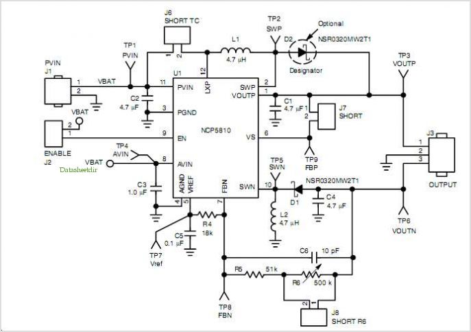
Ncp5810d: Dual 1 W Output Amoled Driver Supply Evaluation Board
The NE568A phase-locked loop (PLL) is designed for high-frequency applications, making it suitable for a variety of communication systems, particularly in satellite technology. The device's operational frequency range, from 1Hz to over 150MHz, allows for versatility in applications ranging from low-frequency demodulation to high-frequency signal processing.
The architecture of the NE568A incorporates several key components that enhance its functionality. The limiting amplifier ensures that the input signal is conditioned correctly for further processing, while the current-controlled oscillator (ICO) allows for fine-tuning of the output frequency, which is essential in maintaining phase alignment with the input signal. The phase detector plays a crucial role in comparing the phase of the input signal with that of the ICO output, thus enabling the PLL to lock onto the desired frequency.
The inclusion of a level shift circuit and voltage/current converters facilitates seamless integration with other circuit elements, allowing for both analog and digital interfacing. The output buffer provides a robust output signal, capable of driving subsequent stages in a communication chain without significant degradation.
The NE568A's temperature compensation features are particularly beneficial in environments where temperature fluctuations can affect performance. The design minimizes the impact of temperature variations on the VCO center frequency, ensuring stable operation across a wide temperature range. This is critical in applications such as satellite communications, where environmental conditions can vary significantly.
The loop filter design is another notable aspect of the NE568A. By allowing configuration with series or shunt elements, the filter can be tailored to optimize the dynamic performance of the PLL, enhancing stability and response time. This flexibility is crucial for applications requiring precise frequency tracking and low distortion in the output signal.
Overall, the NE568A is a highly capable device that combines advanced features with ease of integration, making it a preferred choice for engineers working on high-performance communication systems. Its availability in both dual in-line and surface-mounted packages further simplifies the design process, accommodating various PCB layouts and manufacturing preferences.The NE568A( NE568AD NE568AN SA568AD SA568AN 0 is a monolithic phase-locked loop (PLL) which operates from 1Hz to frequencies in excess of 150MHz and features an extended supply Voltage range and a lower temperature coefficient of the VCO center frequency in comparison with its predecessor, the NE 568. The NE568A is function and pin-compatible with the NE568 requiring only minor changes in peripheral circuitry. Temperature compensation network is different, no resistor on Pin 12, needs to be grounded and Pin 13 has a 3. 9 kOhm resistor to ground. Timing cap, C2, is different and for 70MHz operation with temperature compensation network should be 16pF, not 34pF as was used in the NE568.
The NE568A has the following improvements: ESD protected; extended Vcc range from 4. 5V to 5. 5V; operating temperature range -55 to 125C (see Signetics Military 568A data sheet); less layout sensitivity; and lower TC of VCO (center frequency). The integrated circuit consists of a Limiting Amplifier a current-controlled Oscillator (ICO), a phase detector, a level shift circuit, V/I and I/V converters, an output Buffer and bias circuitry with temperature and frequency compensating characteristics.
The design of the NE568A is particularly well-suited for demodulation of FM signals with extremely large deviation in systems which require a highly linear output. In satellite receiver applications with a 70MHz IF, the NE568A will demodulate, 20% deviations with less than 1.
0% typical non-linearity. In addition to high linearity, the circuit has a loop Filter which CAN be configured with series or shunt elements to optimize loop dynamic performance. The NE568A is available in 20-pin dual in-line and 20-pin SO (surface mounted) plastic packages. 🔗 External reference
Related Circuits
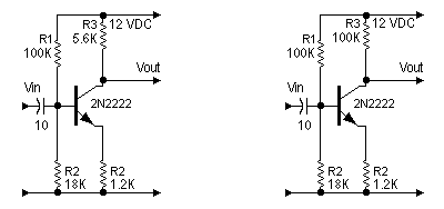
An input sine wave applied to the left amplifier base results in the collector output fluctuating above or below 6.6 volts. The amplifier amplifies and inverts the signal, maintaining a roughly centered output, thereby minimizing the chances of clipping....
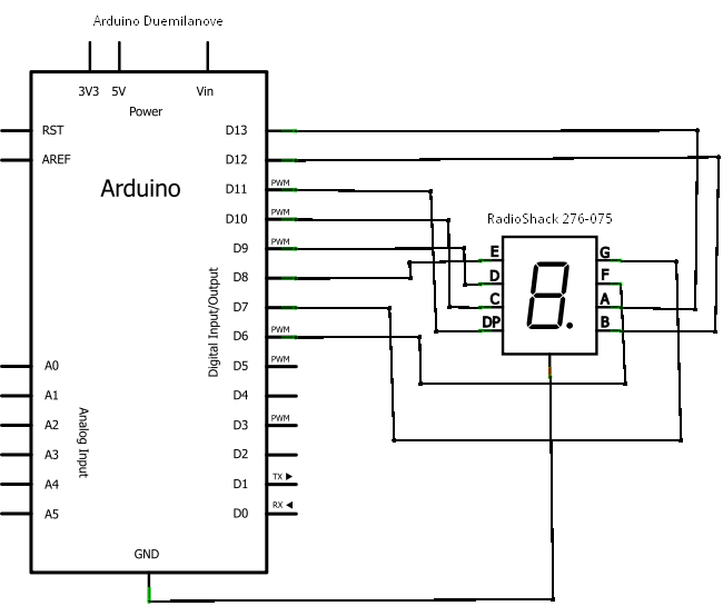
If you're not familiar with the Arduino, it is an open-source electronics prototyping platform based on flexible, easy-to-use hardware and software. It has a small microcontroller, a USB port to connect to your computer for programming, a power socket...
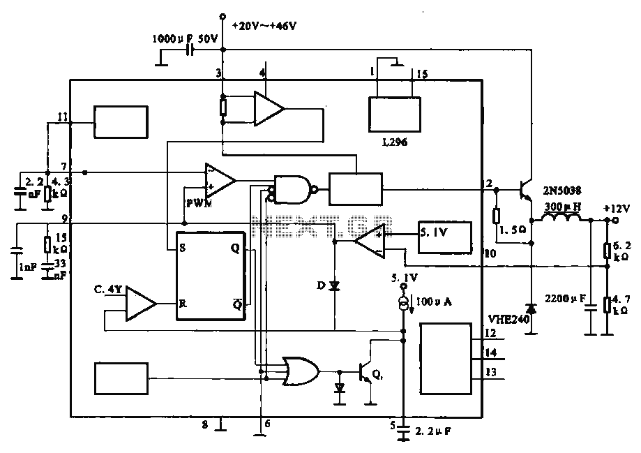
The circuit outputs 12V at 10A and utilizes a high-current switching power supply design based on the L296 component. This configuration allows for an output current of up to 10A, and the entire circuit is compact with minimal component...
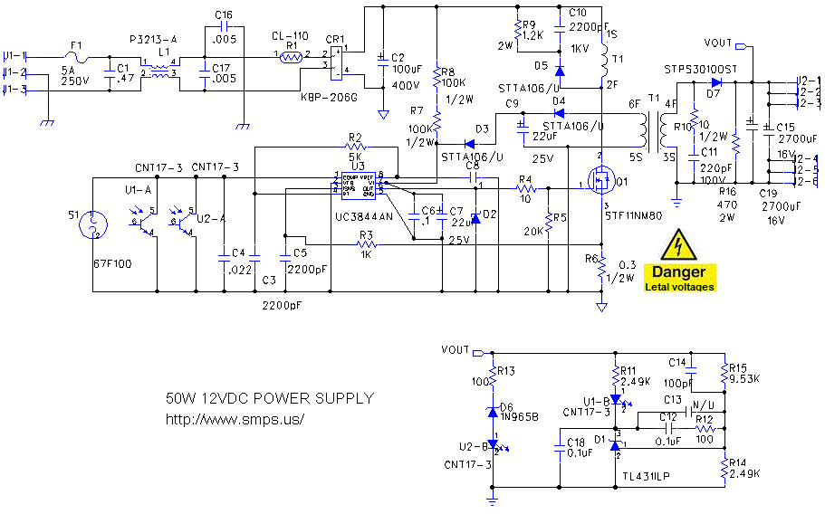
The schematic diagram below illustrates a simple and cost-effective 12-volt DC 50W off-line SMPS (switched-mode power supply) circuit. It is suitable for DIY home projects or for learning about the operation of flyback converters. This power supply unit (PSU)...
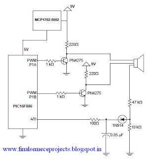
A horn driver project developed by Microchip Technology is illustrated in this circuit diagram. This horn driver project utilizes the PIC16F886 microcontroller from Microchip. The circuit diagram for the PIC microcontroller horn driver is straightforward and requires minimal external...
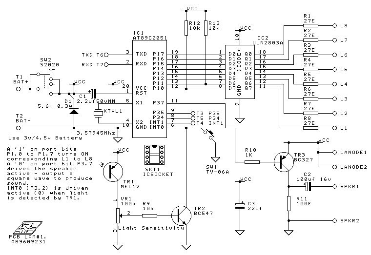
This document describes the HSETI PCB. This PCB is a small simple application for the Atmel AT89C2051 microprocessor - a 20 pin 8051 variant, with FLASH (reprogrammable) program memory. The board has just two chips on it, the CPU...