
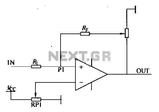
Negative Voltage Reference Circuit

The adjustable voltage reference circuit typically consists of a zener diode, which establishes a stable reference voltage, and an adjustable resistor (R1) that allows for fine-tuning of the output voltage (VOUT). The zener diode is selected based on its voltage rating and temperature characteristics, ensuring that it operates within its optimal range to maintain accuracy across varying temperatures.
In practical applications, the circuit is designed to minimize variations in output voltage due to changes in temperature, which is a critical factor in high-precision environments. The selection of R1 is crucial; it must be chosen carefully to provide the necessary zener current (IZ) that ensures the zener diode operates in its breakdown region, thus achieving the desired output voltage stability.
The schematic representation of the circuit typically includes the zener diode connected in reverse bias, with the adjustable resistor R1 in series with the output. Additional components such as capacitors may be included to filter noise and enhance stability. The output voltage can be measured across R1, and adjustments can be made to achieve the required voltage level while maintaining low temperature coefficients.
Overall, this adjustable voltage reference circuit is essential for applications requiring precise voltage regulation and stability across a wide range of operating conditions.This circuit is a Adjustable voltage reference circuits, a voltage source which provides a voltage greater than the reference diode. High precision extended temperature applications of the circuit require that the range of adjustment of VOUT be restricted.
When this is done, R1 may be chosen to provide optimum zener current for minimum zener T. C. Since IZ is not a function of V+, reference T. C. will be independent of V+. Here is a schematic drawing : 🔗 External reference
Related Circuits
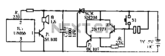
A few custom integrated circuits began to play music. When the song ends, no electricity flows through the thyristor, which then cuts off the light, causing the phototransistor to activate. The system is designed with a touchpad; each touch...
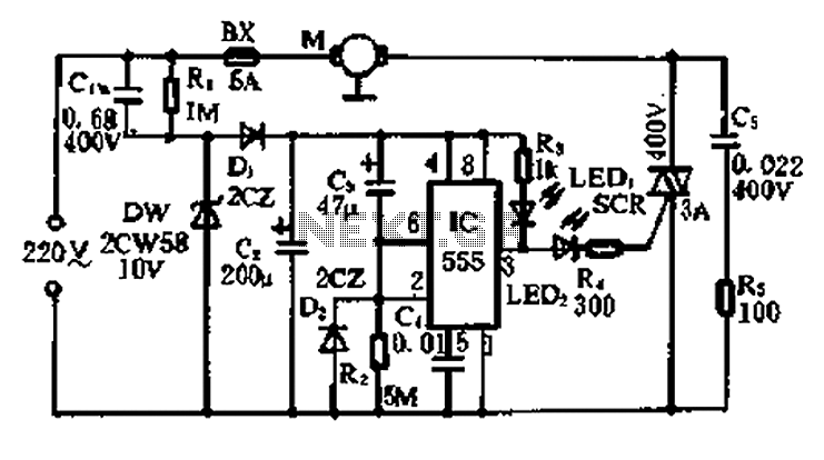
A 5-minute circuit can continue to operate during a power outage, providing protection for the refrigerator. The refrigerator power protection circuit, designated as 1136, includes a power transformer that converts 220V voltage through a rectifier bridge (VD1). This setup...

This circuit generates sine and square wave signals with frequencies ranging from below 20 Hz to above 20 kHz. The advantage of this circuit diagram is that the output frequency can be adjusted by varying the variable resistor R6. The...
Environmental interference can affect the transfer switching, leading to the production of burrs in confidence disgrace. The switch position signal will control the computer system with the reliability of lanthanum burrs. The work has some impact. Glitches are typically...
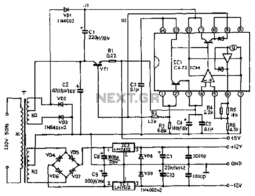
The circuit depicted features a secondary N3 center tap transformer (T) with a common point connecting diodes VD2 and VD3 to positive electrodes, along with capacitors C2, C6, C7, and negative electrodes connected to capacitors C9 and C10. Additional...
The objective is to vary two voltages, V1 and V2, by an equal percentage of their respective ranges (V1MAX - V1MIN and V2MAX - V2MIN), where V1MAX, V1MIN, V2MAX, and V2MIN are independent of one another. A common approach...