
No-bias L-C High-Frequency Oscillator
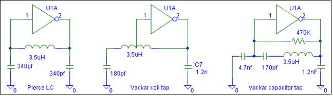
The oscillator circuit utilizing the 74HCU04 hex inverter presents a robust and efficient design for generating stable frequencies in various applications. The choice of the HCU04 allows for a compact layout, minimizing the number of components while maintaining effective performance. The LC resonator configuration benefits from the inherent characteristics of the HCU04, such as its linear amplification capabilities when properly biased.
The design considerations for the oscillator include ensuring that the inverter operates within its linear range to avoid distortion, which can be critical for maintaining signal integrity in clocking applications. The feedback mechanism employed in the Vackar oscillator design is particularly advantageous, as it allows for reactive components to control oscillation without the need for resistive biasing, leading to improved efficiency and reduced power consumption.
In optimizing the circuit, attention must be paid to the quality factor (Q) of the inductor and the overall impedance matching between the resonator and the inverter to ensure maximum energy transfer and stability of the oscillation. The use of a tapped inductor for feedback provides flexibility in tuning the frequency response of the oscillator while maintaining the desired output characteristics.
Overall, the oscillator design utilizing the 74HCU04 hex inverter and LC resonator configuration exemplifies an effective approach to generating stable frequencies with minimal component count, making it suitable for various digital clocking applications and other electronic circuits requiring precise timing signals.This oscillator requires no biasing components. Only an inductor and various matching or tuning capacitors are required to set the operating frequency. The active element is the 74HCU04 hex inverter. Only one of the six inverters is required for the oscillator another may be used as a buffer. A few oscillator circuits are presented, including design procedures. Most HCMOS gates are buffered . In the case of buffered inverters like the 74HC04, a single inverter is constructed from three cascaded inverters. The HCU04 is much simpler with each inverter composed of one enhancement NMOSfet and one PMOSfet in totem-pole configuration.
The NMOSfet`s gate and PMOSfet`s gate are tied together at the input pin, and their drains are tied together at the output pin. When biased mid-way between supply (Vcc) and ground, this structure is a reasonably linear amplifier.
Open-loop gain is measured at 12. 5, with transconductance 0. 023 amps/volt. Output impedance measures 557 ohms. All are dependent on supply voltage (from a Philips data sheet): Since an oscillator`s input or output voltage will be swinging over a considerable range of the 5v supply voltage, the non-linear characteristics of the amplifying inverter have significant influence over the AC operating amplitude. Swings above Vcc or below ground are clamped by internal diodes and can cause latch-up of the device.
Operation too close to the rails should be avoided. The onset of non-linearity such as reduced transconductance or reduced output impedance serve as the mechanism by which amplitude is stabilized every oscillator employs similar means of amplitude control. Of the basic oscillator types, the non-inverting types such as Hartley or Colpitts are not achievable with a single HCU04 amplifier.
Pierce and Vackar are two described here. The Pierce variation using a crystal in place of the inductor, is a popular one used to clock many digital circuits. A resistor is added (between input pin and output pin) to bias the inverter as a linear amplifier. An extra series resistor is sometimes added to limit the power flowing through the crystal. In the simple LC resonator version, it is not possible to match the resonator impedance to amplifier.
A Vackar oscillator is often seen using a depletion FET as the amplifier. It is quite appropriate with an HCU04 substituted. Circulating current in the LC resonator is not limited as it is with a crystal. It is easy to match the HCU04 output impedance to the resistive part of the resonator. A fraction of the resonator voltage is fed back out-of-phase to the HCU04 input. This can be done two ways: with a capacitive voltage divider (as in the conventional Vackar FET circuit), or with a tap on the resonating inductor. The tapped inductor is most attractive, resulting in an oscillator having no resistive biasing components only reactive resonating or matching components.
These Vackar circuits can be easily optimized for nearly any LC components. Upon power-up, oscillator amplitude will increase until the HCU04 becomes non-linear. Since it will self-bias mid-way between ground and supply voltage (+5v nominal), output voltage will swing over some fraction of 5v p-p. At the mid-bias point, transconductance and output resistance is highest: 22mA/V and 500 ohms respectively.
This is the starting point for design. Resonator Q is mostly determined by the inductor Q. A 3. 5uH inductor was wound onto a T50-2 toroid core (25 turns of #22 magnet wire). Its unloaded Q @ 7MHz. was 170. The output shunting capacitor is chosen to match the HCU04`s 500 ohm output resistance to the inductor`s 0. 9 ohm series resistance. Capacitive reactance required is about 1200 pf. If we assume that output swing is about 3v p-p, total resonator voltage across the inductor will be close to 25 v p-p.
A 170 pF resonating capacitor is required at the hot end. The hot end will swing with opposite phase compared to the driv 🔗 External reference
Related Circuits
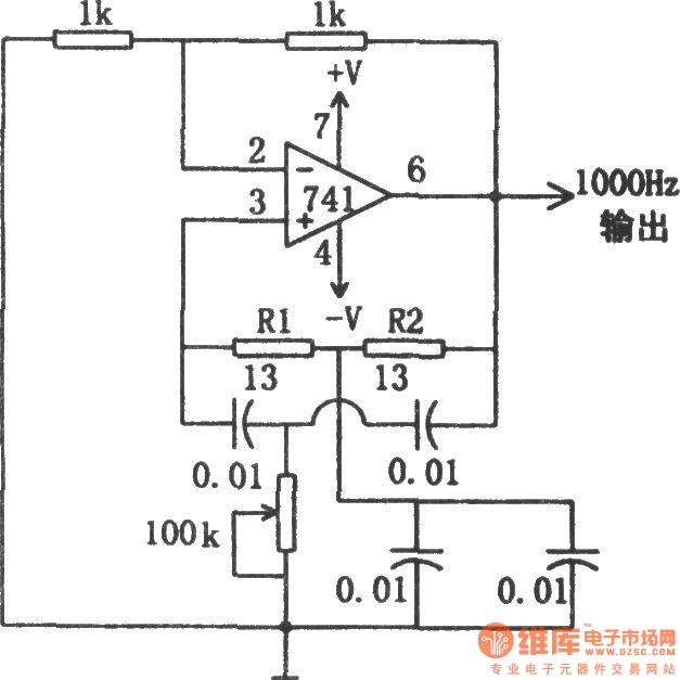
The circuit illustrated in the diagram is a 1 kHz sine wave oscillator circuit. Based on a double-T circuit configuration, it utilizes a standard 741 operational amplifier to generate a 1000 Hz sine wave output. The circuit begins oscillation...
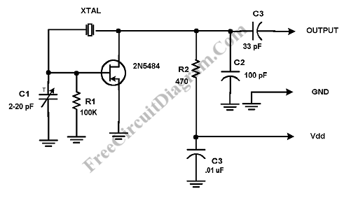
This circuit is a conventional Pierce type oscillator that utilizes a JFET. It employs fundamental mode crystals and demonstrates decent performance and reliability. The Pierce oscillator is a popular configuration for generating stable oscillations, particularly in applications requiring a stable...
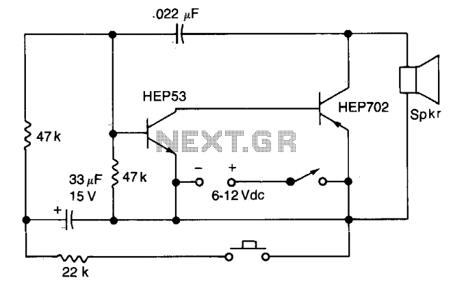
Closing the pushbutton switch initiates the siren, which then increases to a higher frequency. Releasing the switch causes the tone to decrease until switch S2 is closed again. The quality of the tone can be modified by altering the...
The initial intention for this posting was to title it "Crystal Oscillator Blues," reflecting the challenges faced in constructing the crystal oscillator for the GPS Disciplined Oscillator (GPSDO), as mentioned in a previous post. However, there have been some...
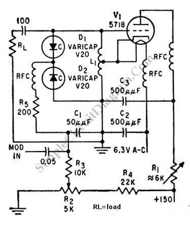
This is a 100 MHz varicap oscillator circuit. It can provide modulation signals of less than 28 V and a frequency deviation of 28 MHz peak-to-peak. The 100 MHz varicap oscillator circuit utilizes a varactor diode, which is a semiconductor...
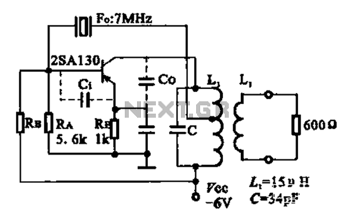
The 2SA130 transistor is used in an oscillator circuit with an oscillation frequency of 7 MHz. The power supply voltage is 6V, and the load is a frequency-selective resonant circuit with a quality factor of 600. The circuit utilizes the...