
No linear feedback amplifier circuit a
The described circuit is a sophisticated arrangement designed to achieve high-performance differential voltage amplification. The differential input stage is crucial for processing small signal variations while rejecting common-mode noise effectively. The use of FETs in the input stage is advantageous due to their high input impedance, which allows for minimal loading on the preceding circuit and improves overall signal integrity.
The forced differential voltage amplification stage enhances the circuit's ability to maintain linearity and reduce distortion, which is vital in applications requiring high fidelity. The design incorporates a bias circuit that stabilizes the operating point of the amplifiers, ensuring consistent performance across varying input conditions. The distortion servo circuit actively monitors and corrects any deviations from the desired output, further enhancing the fidelity of the amplification process.
The common-emitter amplifier configuration provides additional gain and improves the bandwidth of the circuit. The inclusion of phase compensation through capacitor C102 is essential to mitigate potential stability issues that could arise from high-frequency signals. The careful selection of components ensures that the circuit remains robust against variations in supply voltage and temperature, thus maintaining performance over a wide range of operating conditions.
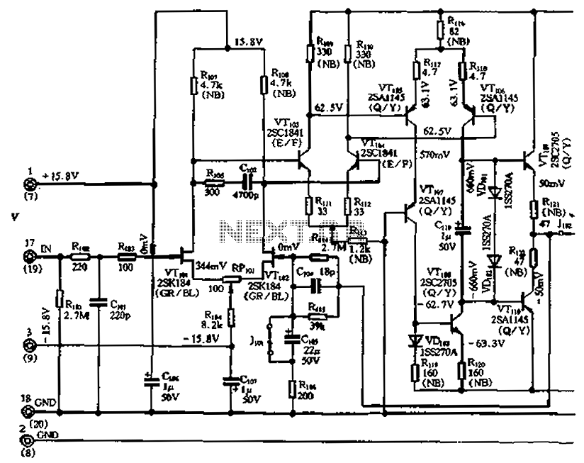
Overall, this circuit exemplifies a well-engineered approach to differential amplification, balancing performance, stability, and simplicity, making it suitable for a variety of electronic applications, including audio processing, sensor signal conditioning, and instrumentation. By the differential input stage, a differential voltage amplification, a forced differential voltage amplification, slow punch amplified complementary push-pull amplifier outpu t bias circuit, distortion servo circuit and protection circuit. Figure 2-41 (a) for the input preamplifier stage. VTioi, VTloz composition FET differential input circuit. Due to the high input impedance FET input for the omitted input capacitance, a real DC amplifier circuit. Due to the low voltage FET, using a single low-voltage power supply ( 15 -8V), and the use of 9m high FET o Rcos, C102 is a phase compensation circuit, to prevent the stop rate is too high due to the input signal distortion.
VTi, VT04 constitute a differential voltage amplifier stage, to get enough gain to drive to force a balanced differential amplifier stage, this level takes a larger operating current t about 4. SMAO VTios ~ VTios constitute very good performance to force balanced differential amplifier level. This circuit is a good solution to the electrical effect of changes in voltage of the differential circuit, and simple circuit design improves the circuit gain, fork reduces distortion.
In VTios collector access, L07 constitute a common-emitter amplifier circuit group altogether, not only can improve the linearity, wide bandwidth the same time, due VTll07 of access makes this group a set level between zero equivalent capacitance, this greatly reduces the level of distortion. VT109, VTiio constituting a buffer amplifier stage, VDiot, VD102 constitutes its base bias circuit, the present stage to provide a bias current of about ImA o cII (J is the base bias stabilizing capacitor, which makes the collector current VT106 the AC component is bypassed, the bias voltage to maintain the output level constant, and the distortion correction circuit.
Related Circuits
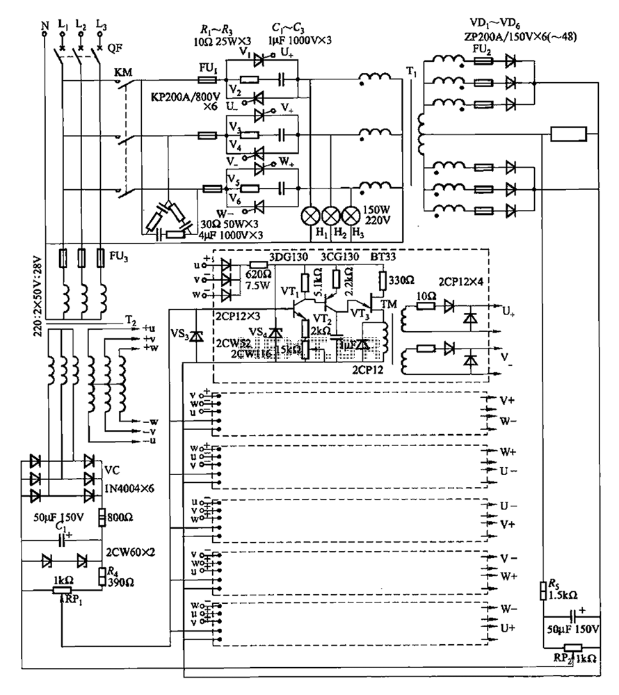
FGDF-3 is a three-phase low-temperature iron plating main circuit, while the KGDF-3 represents a low-temperature iron plating power supply device that includes characteristics of a single-phase low-temperature iron plating power supply. This device utilizes a three-phase power grid to...
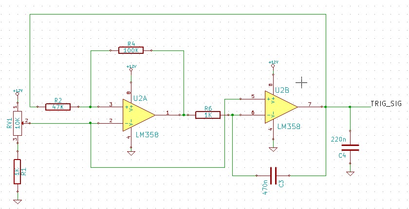
This circuit utilizes LM358 operational amplifiers (or any single supply operational amplifier) to generate a pulse-width modulated (PWM) signal. The design was specifically created for a local marine repair company that requested a circuit that is easily repairable and...

R1 is a 15k ohm resistor. An NTC thermistor rated at 10k ohm, available at Radio Shack in the United States, is utilized. P1 is a 10k ohm potentiometer that sets the low speed (voltage) of the fans at...
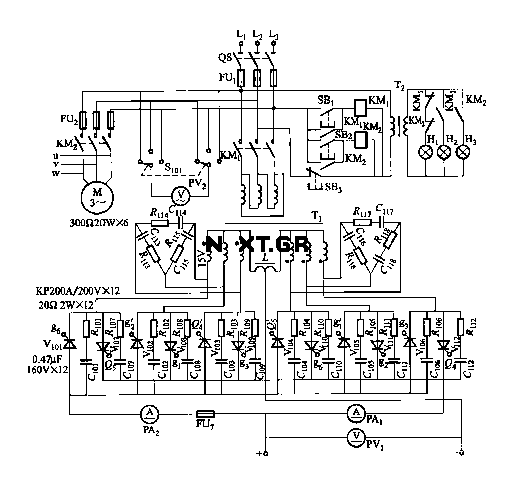
A three-phase thyristor power regulator circuit designed for plating applications, capable of handling currents from 1200A to 6000A at a voltage of 10V. The circuit comprises a main circuit, a trigger circuit, synchronous power components, and a voltage negative...
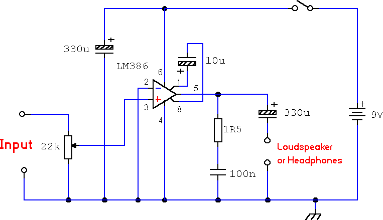
A compact 325mW amplifier with a voltage gain of 200, suitable for use as a bench amplifier, signal tracer, or to amplify the output from personal radios. The circuit utilizes the National Semiconductor LM386 amplifier. In the schematic, the...
There are monitors that feature only three BNC inputs and utilize composite synchronization (sync on green). This circuit has been specifically designed for such monitors. The design maintains simplicity while delivering reasonable performance. The operational principle is straightforward. The...
Warning: include(partials/cookie-banner.php): Failed to open stream: Permission denied in /var/www/html/nextgr/view-circuit.php on line 713
Warning: include(): Failed opening 'partials/cookie-banner.php' for inclusion (include_path='.:/usr/share/php') in /var/www/html/nextgr/view-circuit.php on line 713