
nokia 5130 keypad ic solution 1000% working
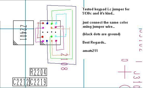
The Nokia 5130 mobile phone features a keypad that can occasionally experience issues due to faulty connections or worn-out components. To resolve these issues, a jumper can be implemented, which involves creating a direct electrical connection on the circuit board that facilitates the keypad's functionality.
The jumper process typically requires careful examination of the circuit board, where the keypad connects to the main processor. A diagram is essential as it provides a visual representation of the specific points on the circuit board that need to be connected. This diagram may indicate the exact locations for soldering the jumper wire, ensuring that the connection is made without disrupting other components.
Once the jumper is placed according to the diagram, it is crucial to test the keypad functionality. A multimeter can be used to check for continuity and ensure that the jumper has been successfully implemented. Following the jumper installation, the keypad should respond correctly to all inputs, confirming that the issue has been resolved. Proper handling and soldering techniques are essential to avoid damaging the circuit board or other components during this process.nokia 5130 keypad jumper just follow the diagram.. tested just now.. after doing the jumper.. all keypads working well .. 🔗 External reference
Related Circuits
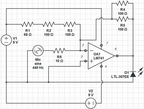
Red = V+, Black = V-, Green = GND, Yellow = Mic Input, Orange = LED Output. The op-amp used is an LM741, which is intended to adjust the peak brightness of the LED based on the ambient sound...

IC1 generates a pulse that modulates the 1000-Hz tone generated by IC2. This circuit can be used to generate warning or alert signals. The circuit described consists of two integrated circuits (ICs), where IC1 is responsible for generating a pulse...

The Keypad must be the kind with a common terminal and a separate connection for each key. On a 12-key pad, look for 13 terminals. The matrix type with 7 terminals will NOT do. The Alarm is set by...
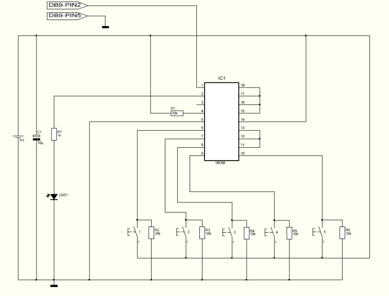
This project can be used for many different purposes. Probably the most used application would be to interface to any electronic project that requires a keypad. There are several ready made keypads on the market, but those work with...
The CDCF5801 provides clock multiplication from a reference clock (REFCLK) signal with the unique capability to delay or advance the CLKOUT/CLKOUTB with steps of only 1.3 mUI through a phase aligner. For every rising edge on the DLYCTRL pin,...
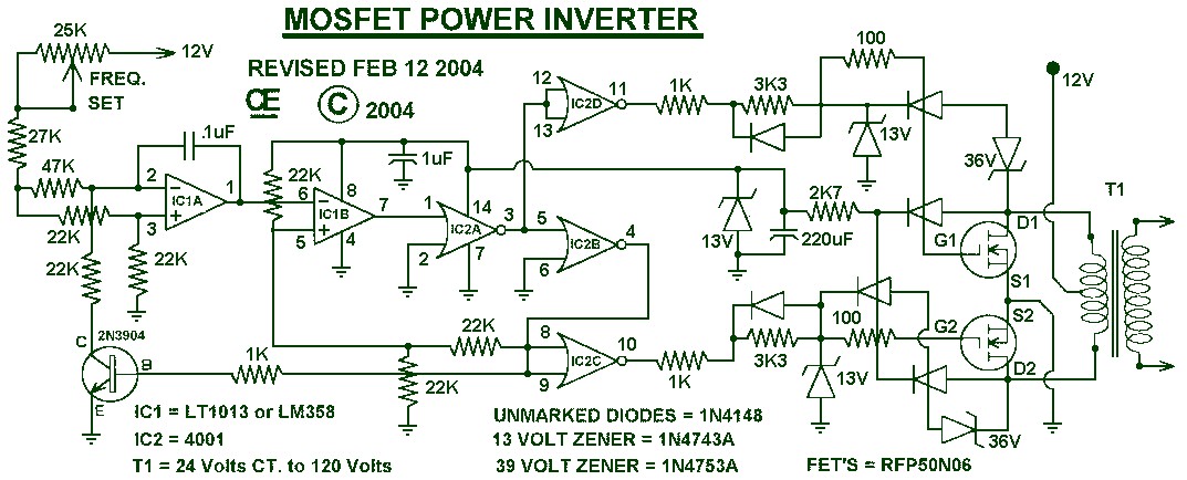
1000W Power Inverter circuit diagram: This is a power inverter circuit based on the MOSFET RFP50N06. The inverter is capable of handling loads up to 1000W, depending on the specifications of the transformer used. The RFP50N06 MOSFETs are rated...