
Noninverting gain circuit diagram by the MAX4107
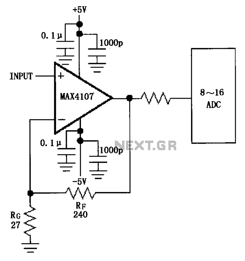
The inverting gain circuit using the MAX4107 operational amplifier is designed to function as an analog-to-digital converter (ADC) input buffer. The circuit configuration allows for the amplification of input signals while maintaining a high input impedance and low output impedance, which is crucial for interfacing with ADCs.
In this configuration, the gain of the amplifier is determined by the feedback resistor (RF) and the input resistor (RG). The relationship governing the gain (Av) of the inverting amplifier is given by the formula: Av = -RF/RG. For this particular design, the resistors are selected such that the gain is set to approximately 10. This means that for every 1V input signal, the output will be -10V, inverting the phase of the signal while amplifying its magnitude.
The choice of RF and RG values must be made carefully to ensure stability and linearity of the amplifier. Additionally, the MAX4107 is known for its low noise and high speed, making it suitable for high-frequency applications. Proper bypass capacitors should be placed close to the power supply pins of the MAX4107 to minimize power supply noise and ensure stable operation.
In summary, this inverting gain circuit effectively amplifies signals for ADC applications, providing a reliable interface with the necessary gain characteristics. As shown in FIG inverting gain circuit from the MAX4107 configured as ADC input buffers. Amplifier gain is determined by the ratio of RF and RG, resistors set the gain figure o f about 10.
Related Circuits
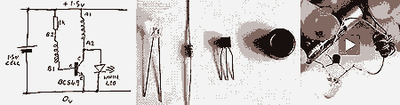
This circuit can be utilized in various devices to extract residual energy from seemingly depleted batteries. It is possible to connect multiple dead batteries in order to maximize energy extraction. This circuit design, often referred to as a Joule Thief,...

A CMOS-based circuit designed for adjusting the time of spot welding. This circuit utilizes a CMOS device that allows for cycle selection ranging from 1 to 99 cycles. In practical applications, most users find that adjustments within 10 cycles...

This design circuit is for a simple 27MHz transmitter that produces a carrier signal. The circuit generates an unmodulated 27MHz signal, which can be received by a compatible receiver. The transmitter operates as a basic crystal oscillator, with the...
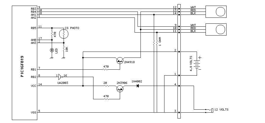
Very little extra circuitry is needed to do both forward and backward walking sequences along with a few other tricks. The PIC16F818 has a lot of features that work well in this situation. As you can see from the...

Personal Safes are revolutionary locking storage cases that open with just the touch of your finger. These products are designed as secure storage for medications, jewelry, weapons, documents, and other valuable or potentially harmful items. These utilize fingerprint recognition...
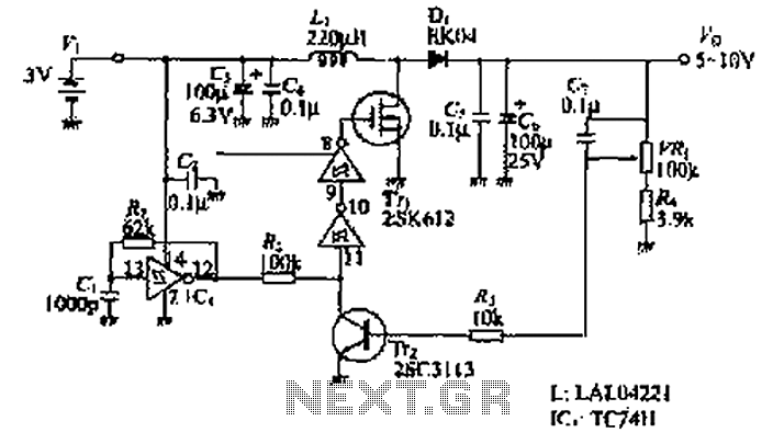
The design of the power supply circuit diagram utilizes an oscillator circuit from the 74HC series of CMOS logic circuits, with a MOSFET as the switching device. This configuration allows for the development of small-scale power supplies suitable for...