
One zero trigger thyristor power adjustment circuit
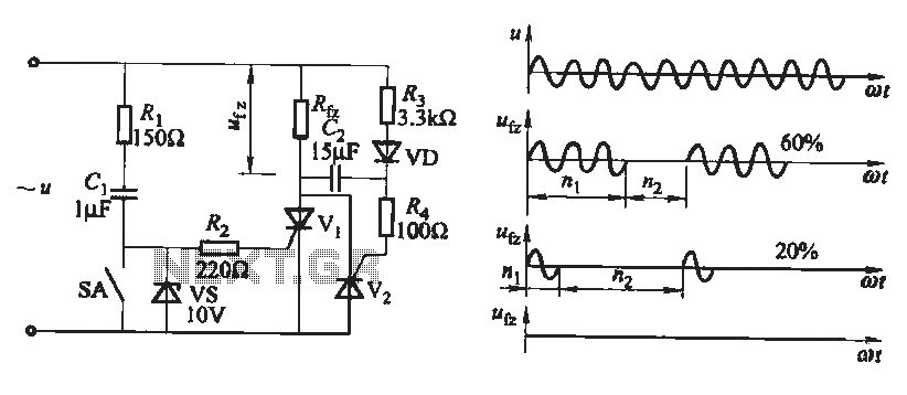
The thyristor zero trigger circuit is designed to provide a stable sine wave output while minimizing electromagnetic interference, making it suitable for applications requiring precise power control. The circuit employs a thyristor, which acts as a switch controlled by the gate current. The clamping action of the regulator is crucial for maintaining the voltage across the capacitor Ci, allowing it to charge efficiently while preventing overvoltage conditions.
The diode VD plays a critical role in ensuring that the capacitor Cz does not discharge negatively, which could lead to damaging reverse currents. By preventing reverse charge during the negative half cycle, the diode ensures the longevity and reliability of the circuit components. The current limiting resistors Rz and R4 are essential for protecting the thyristor and other components from excessive current, which could cause thermal runaway or failure.
The timing of power outages is a significant feature of this circuit, as it allows for controlled power delivery to the load. The time bar switch SA provides a means to adjust the duration of the power supply, effectively controlling the load power. This feature can be particularly useful in applications that require variable power levels or in systems where load conditions may change frequently.
In summary, the thyristor zero trigger circuit is an effective solution for achieving controlled sine wave output with minimal interference, utilizing key components such as regulators, diodes, and resistors to ensure stable operation and protection against adverse conditions. The design emphasizes reliability and adaptability, making it suitable for various electronic applications.Thyristor zero trigger circuit output waveform is a sine wave, it will not produce as phase-shift trigger circuit as electromagnetic interference. This is a zero trigger thyristor power adjustment of the basic circuit. The figure, the regulator vs plays clamping action and to provide access to the charging capacitor Ci; VD role is to prevent the negative half cycle of the power supply capacitor Cz reverse charge; resistance Rz and R4 are current limiting resistor to limit the control current. Figure, power outage time digging 1 and 2 depending on the time bar switch length (or control contact) SA opening and closing time.
That load power by the SA control.
Related Circuits
This simple low voltage tester circuit can be used to monitor batteries and other voltage sources for issues, utilizing an LED display and alarm sound. The low voltage tester circuit is designed to provide a reliable method for monitoring the...
One of the most effective communication methods to be implemented in a digital system is the use of the RS232 serial line. The microcontroller 89S51 is equipped with a UART, allowing it to perform serial communication at RS232 levels...
This system operates on the principle that the capacitance loading of an oscillator will lower its frequency. When a foreign body comes into contact with the touch plate, the frequency of U1 is lowered. This removes the oscillator signal...
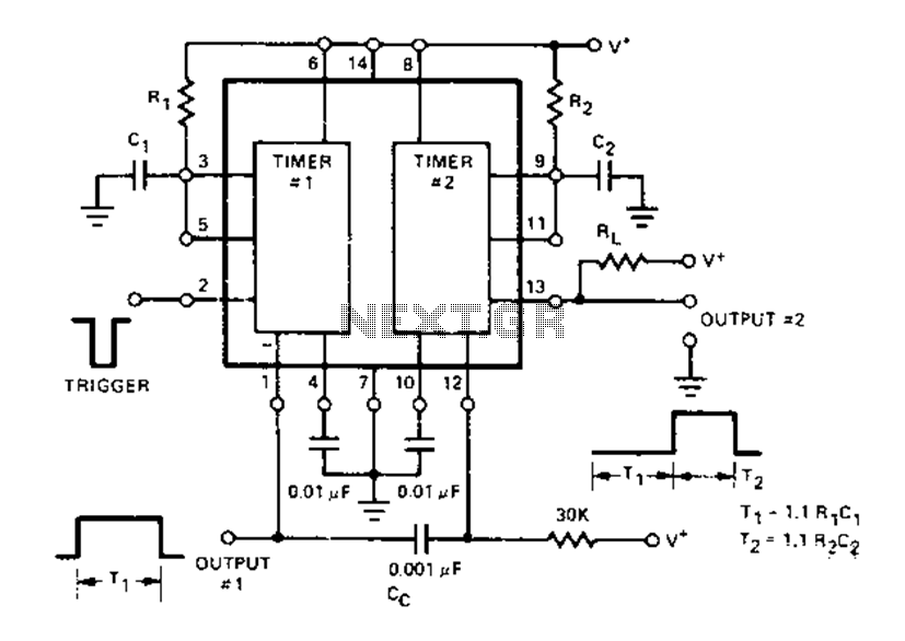
The Dual Timer Exar XR-2556 features a timing mechanism that can be triggered through capacitive coupling on a secondary timing pin. When a trigger input is engaged, the duration T1 can be set to 1.1R1C1, resulting in an increased...
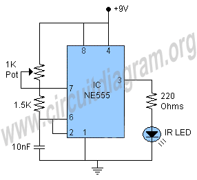
This schematic illustrates an infrared (IR) transmitter circuit utilizing an integrated circuit (IC). The circuit employs the widely recognized NE555 timer IC, which operates as an astable multivibrator to generate a signal with a frequency of 38 kHz. The...
The Zener diode may not be providing sufficient current in its breakdown state to activate the transistor. Removing resistor R2 did not resolve the issue. The Zener's voltage selection could be too high, potentially preventing it from regulating the...
Warning: include(partials/cookie-banner.php): Failed to open stream: Permission denied in /var/www/html/nextgr/view-circuit.php on line 713
Warning: include(): Failed opening 'partials/cookie-banner.php' for inclusion (include_path='.:/usr/share/php') in /var/www/html/nextgr/view-circuit.php on line 713