
Oscillator circuit diagram with triangle-wave/square wave output
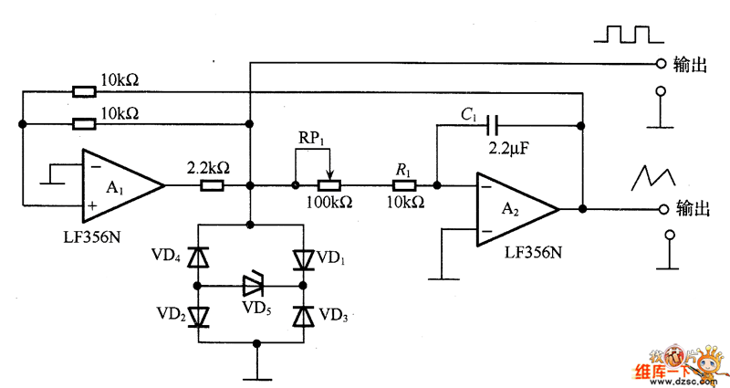
The described circuit operates as a lag comparator integrated with an inverting integrator, which is essential for generating a specific output waveform in response to input signals. The lag comparator, represented by amplifier A1, is designed to compare input voltage levels and provide a corresponding output that reflects the delay in response. The inverting integrator, represented by amplifier A2, takes the output from the lag comparator and integrates it over time, producing a voltage that is proportional to the integral of the input signal.
The time constants for charging and discharging within this circuit are critically defined by the resistors (R1 and RP1) and the capacitor C1. The total resistance (R1 + RP1) determines how quickly the capacitor can charge and discharge, thereby influencing the overall response time of the circuit. A longer time constant results in a slower response, while a shorter time constant allows for a quicker response to changes in the input signal.
Diodes VD1 to VD5 are configured to form a limiter circuit, which serves to protect the subsequent stages of the circuit from voltage levels that exceed specified thresholds. This limiter circuit ensures that the output waveform remains within safe operating limits, preventing damage to sensitive components and maintaining signal integrity.
The maximum oscillation frequency of the circuit is closely tied to the switching rate of the amplifier. With a switching rate of 10V/µs, the circuit is capable of achieving a peak-to-peak output voltage of 20V. This relationship between switching rate and output voltage is crucial for applications that require rapid signal processing and precise control over voltage levels. The design considerations for this circuit are particularly important in high-speed applications where timing and voltage thresholds must be tightly controlled.The circuit is composed of lag comparator with A1 and inverting integrator A2, and the charging and discharging time constant is decided by integral resistors (R1+RP1) and the capacitor C1. VD1~VD5 form the limiter circuit. The maximum oscillation frequency is related to swicthing rate of amplifier, when swicthing rate is 10V/?
s, in order to get the 20V (p.. 🔗 External reference
Related Circuits
This example presents a switch DC regulated power supply circuit designed for buck-mode +5V applications. It consists of a power supply circuit, an impulsator, a voltage sampling or pulse width modulation circuit, and a buffering driver circuit, as illustrated...
Its state is constantly changing, and this change affects the flow of current and voltage, which is visible with the two LEDs. The speed of the LED flasher can be adjusted with potentiometer P1. As an astable multivibrator, the...
This is a simple schematic designed to control a lamp using a Sony TV remote control. The circuit employs a PWM signal connected to a photocoupler, which isolates the power section from the microcontroller. The power section features an...
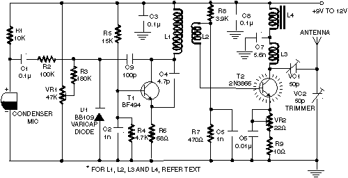
The transmitter described here includes an additional RF power amplifier stage following the oscillator stage, which increases the output power to 200-250 milliwatts. When connected to a properly matched 50-ohm ground plane antenna or a multi-element Yagi antenna, this...
Six timing positions suited to different skin types; timing affected by sunlight intensity. This timer was designed for individuals seeking to achieve a tan. The electronic timer circuit described is intended for use in tanning applications, specifically designed to cater...
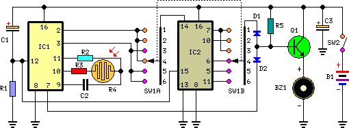
This light-dependent sensor utilizes light-dependent resistors (LDRs) to detect the presence or absence of light. The alarm remains inactive as long as the light source illuminating the LDRs is constant. However, if the light is interrupted, the alarm is activated. The...
Warning: include(partials/cookie-banner.php): Failed to open stream: Permission denied in /var/www/html/nextgr/view-circuit.php on line 713
Warning: include(): Failed opening 'partials/cookie-banner.php' for inclusion (include_path='.:/usr/share/php') in /var/www/html/nextgr/view-circuit.php on line 713