
7 MHz VFO


The resonant LC circuit can also be tuned to the second, third or fourth harmonic. For an improved signal shape however, an extra tuned amplifier stage is necessary. With this adjustment the oscillator is capable for use on 20 meters (14000-14070 KHz), 15 meters (21000-21105 KHz) or 10 meters (28000-28140 KHz). You can build a power oscillator with an NE592 and some additional parts. Depending on the crystal frequency, RF power generation in the range of 1 to 30 MHz is possible. The parallel resonant circuit C1/L1 must be tuned exactly to the crystal frequency. For final transistors one can use two 2N3906 or BS250 (see QRP push-pull amplifier). RF power output can be adjusted from 20 mW to 1.5 W by varying a common emitter resistor in the push-pull stage. Do not use this circuit as a transmitter. When keying the NE592 power supply (pin 3) frequency variation (chirp) occurs. If you insist on transmitting with this circuit, then switch the final transistors directly. To do this put a 10 uH choke in series with the key and a 0.1 uF capacitor in parallel. Disadvantages of this circuit are the NE 592 quiescent current (18 mA), the continuously working oscillator and the hard keying.
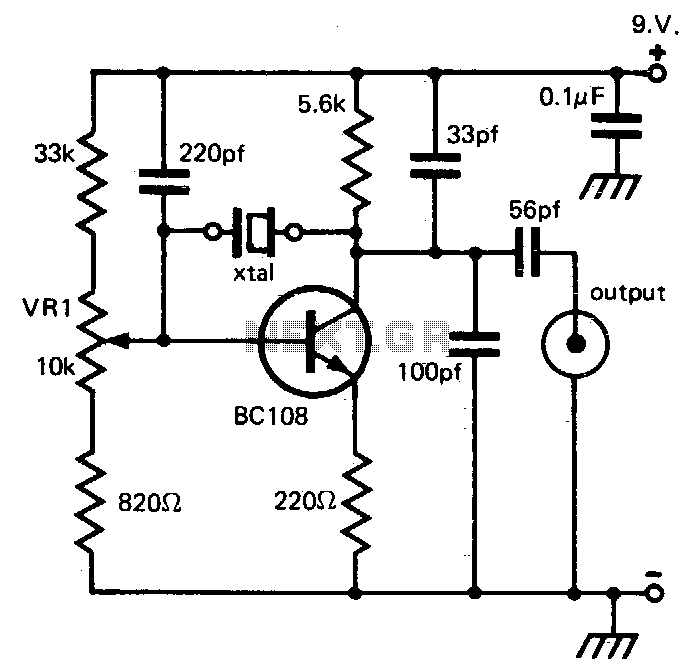
This description outlines a 7 MHz oscillator utilizing a variable crystal oscillator (VXO) and a ceramic resonator for improved frequency stability and tuning capability. The oscillator's design allows for a frequency variation of approximately 35 kHz, effectively bridging the gap between the stability of a VXO and the broader tunability of a variable frequency oscillator (VFO). The resonant LC circuit positioned at the collector of transistor VT1 serves dual purposes: it enhances the output signal shape and mitigates amplitude drops that occur near the frequency of 7020 kHz.
To achieve optimal performance, the resonant LC circuit must be meticulously adjusted to yield a maximum output amplitude of 2Vss at 7035 kHz. A regulated voltage supply of +6 V is essential for the oscillator's proper functioning. Furthermore, this design allows for harmonic tuning, enabling the circuit to operate effectively on various amateur radio bands, including the 20-meter, 15-meter, and 10-meter bands.
The integration of the NE592 operational amplifier facilitates the construction of a power oscillator capable of generating RF power across a frequency range of 1 to 30 MHz, contingent upon the selected crystal frequency. The parallel resonant circuit comprising components C1 and L1 requires precise tuning to match the crystal frequency to ensure efficient operation. For the output stage, transistors such as the 2N3906 or BS250 can be employed in a push-pull configuration, allowing for adjustable RF power output ranging from 20 mW to 1.5 W by modifying the common emitter resistor.
It is important to note that this circuit is not intended for use as a transmitter due to potential frequency chirping when the NE592 power supply is keyed. For those who choose to transmit, it is recommended to directly switch the final transistors, incorporating a 10 µH choke in series with the key and a 0.1 µF capacitor in parallel to mitigate unwanted frequency variations. The design does have limitations, including the NE592's quiescent current of 18 mA and the continuous operation of the oscillator, which may lead to hard keying issues.A 7 MHz oscillator with a variable crystal oscillator (VXO) operates very stably, but it allows only a small frequency variation (approx. 5 kHz). In contrast, a VFO with an LC resonant circuit can be tuned over a range of several hundred kHz, but its frequency stability will depend upon its construction.
The use of a ceramic resonator as frequency-determining component fulfills both requirements. The following oscillator circuit, which uses a ceramic resonator, offers a tuning range of 35 kHz with good frequency stability. The somewhat unusual resonant LC circuit at the collector of VT1 has two functions. It improves the shape of the output signal and at the same time compensates the amplitude drop starting at approximately 7020 kHz.
The transfer characteristic of the ceramic resonator gives this effect. The resonant LC circuit must be adjusted for maximum output amplitude (2Vss) at 7035 kHz. The oscillator needs a regulated voltage of +6 V for proper operation. The resonant LC circuit can also be tuned to the second, third or forth harmonic. For an improved signal shape however, an extra tuned amplifier stage is necessary. With this adjustment the oscillator is capable for use on 20 meters (14000-14070 KHz), 15 meters (21000-21105 KHz) or 10 meters (28000-28140 KHz). You can build a power oscillator with an NE592 and some additional parts. Depending on the crystal frequency, RF power generation in the range of 1 to 30 MHz is possible. The parallel resonant circuit C1/L1 must be tuned exactly to the crystal frequency. For final transistors one can use two 2N3906 or BS250 (see QRP push-pull amplifier). RF power output can be adjusted from 20 mW to 1.5 W by varying a common emitter resistor in the push-pull stage.
Do not use this circuit as a transmitter. When keying the NE592 power supply (pin 3) frequency variation (chirp) occurs. If you insist on transmitting with this circuit, then switch the final transistors directly. To do this put a 10 uH choke in series with the key and a 0.1 uF capacitor in parallel. Disadvantages of this circuit are the NE 592 quiescent current (18 mA), the continuously working oscillator and the hard keying. 🔗 External reference
Related Circuits
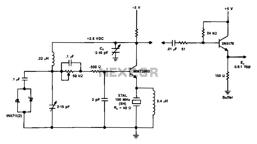
The diagram illustrates a 100 MHz oscillator functioning on the fifth harmonic. To preserve the transistor's gain, it is important to note the increase in the collector's load resistance, Rl, due to the rise in the quartz crystal's internal...
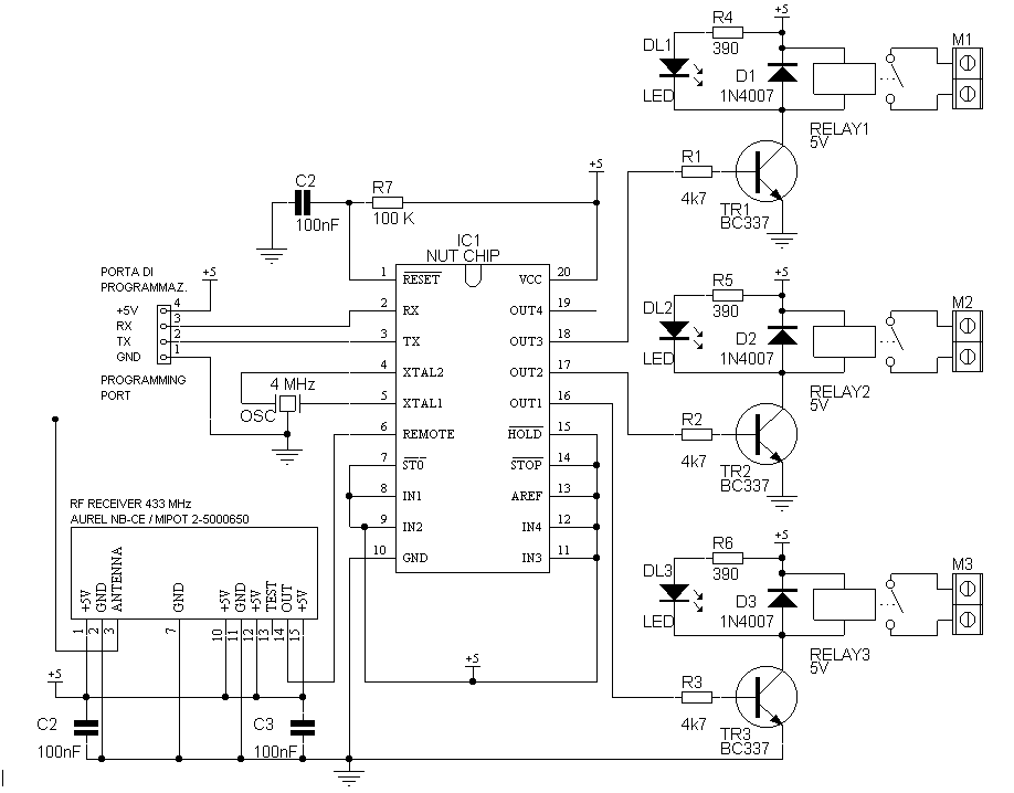
The schematic is very simple and includes, in addition to Nutchip, with its three driving transistor and LED, the radio receiver. The data come from the OUT pin of the receiver and enter the pin REMOTE remote control. The...
A wide range frequency meter is a useful tool for an electronics lab. This project describes a frequency meter based on the AT90S231 microcontroller that can measure input frequencies up to 50 MHz. The measured frequency is displayed on...
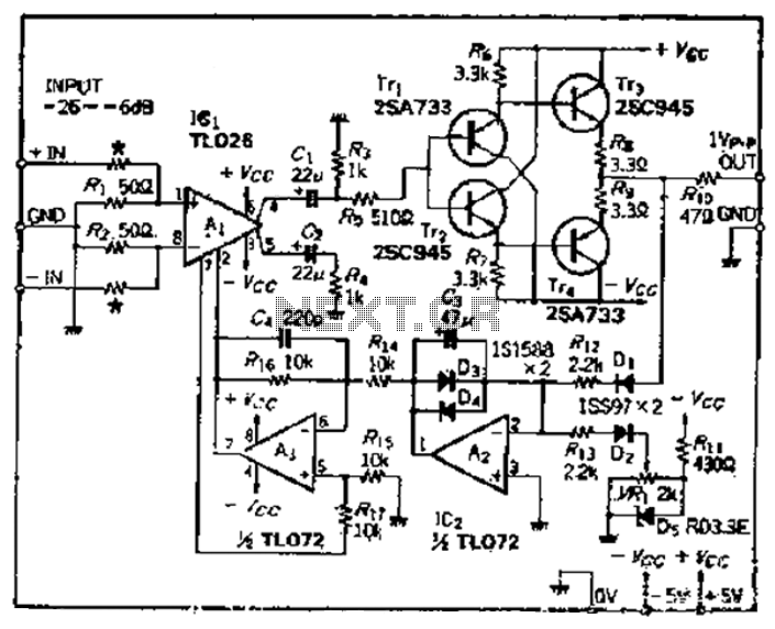
A car circuit is utilized for external voltage-controlled amplification in wideband amplifiers using the TL0216 IC. This design incorporates compression characteristics of 2dB. The input circuit consists of resistors that reduce the input level when it is between -26dB...
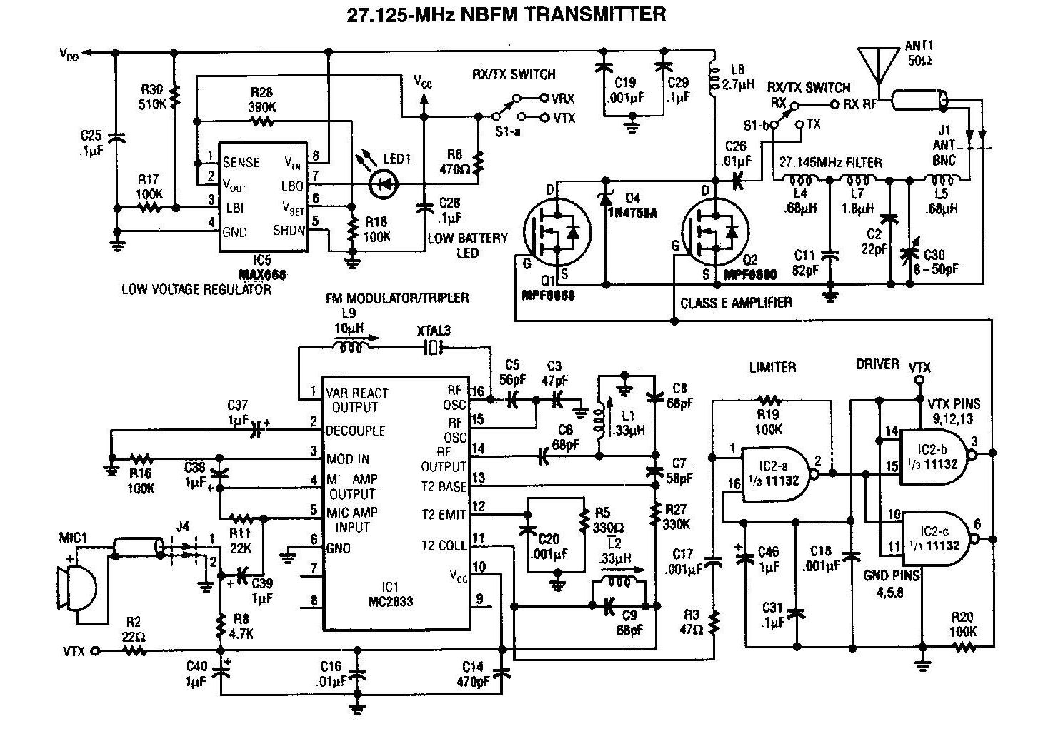
A 27MHz transmitter circuit schematic utilizing the MC2833 and two FET transistors, MPF6660. This design incorporates a Motorola MC2833 one-chip FM transmitter along with several supporting components. The 27MHz transmitter circuit is designed to operate within the FM radio frequency...
This circuit provides reliable oscillation and an output close to one volt peak-to-peak. Power consumption is around 1 mA from a nine-volt supply. The described circuit is likely a simple oscillator designed to generate a periodic waveform with a peak-to-peak...