
Oscilloscope triggered sweep circuit
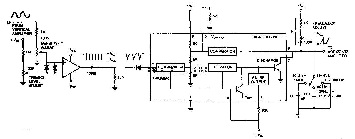
The described circuit utilizes an operational amplifier (op-amp) as a comparator, which plays a critical role in controlling the timing sequence. The op-amp compares the voltage across capacitor C with a reference voltage equivalent to 0.33 times the supply voltage (Vee). When the input voltage from the op-amp exceeds this threshold, it triggers the timer circuit, which is typically configured using a monostable or astable multivibrator configuration.
The timer's output is connected to a flip-flop, which serves to maintain the state of the circuit during the timing interval. When the flip-flop is set, it disables the discharge transistor, allowing capacitor C to charge through a designated charging path. The charging time is determined by the RC time constant, where R is the resistance in series with the capacitor, and C is the capacitance value.
Once the voltage across the capacitor reaches the specified control voltage, the flip-flop resets. This action enables the discharge transistor, which creates a path for the capacitor to discharge rapidly. The discharge path is crucial for resetting the circuit to its initial state, allowing for subsequent cycles of operation.
To enhance the linearity of the timing behavior, a constant-current source can be introduced in place of the variable resistor R used for frequency adjustment. This modification ensures that the charging current remains stable, resulting in a more predictable and linear voltage rise across the capacitor. Such an improvement is particularly beneficial in applications requiring precise timing intervals and consistent performance across varying conditions.
Overall, this circuit design effectively demonstrates the interplay between analog components, providing a reliable method for timing applications while allowing for adjustments to optimize performance characteristics.The circuit"s input op amp triggers the timer, sets its flip-flop and cuts off its discharge transistor so that capacitor C can charge. When capacitor voltage reaches the timer"s control voltage of 0.33 Vee. the flip-flop resets and the transistor conducts, discharging the capacitor.
Greater linearity can be achieved by substituting a constant-current source for frequency adjust resistor R.
🔗 External referenceRelated Circuits
In the previous post, the primary principles of the switching power supply were discussed. Essentially, an oscillator drives a transformer with a ferrite core at a relatively high frequency, thereby minimizing the size, weight, and cost of power supplies....
This simple logarithmic amplifier circuit uses the LT1012, which has a low bias current that allows for 4.5 decades of voltage input logging. Additionally, transistors that can be used in this circuit include the 2N2979. The logarithmic amplifier circuit designed...
The digital scoreboard circuit is designed to display numerical values ranging from 0 to 9 on a common anode 7-segment display. The circuit employs a 7-segment driver integrated circuit (IC), specifically the 74LS47 or 74LS247. A 555 timer IC...
A circuit was constructed based on an LED beating heart frame instructable, but it is not functioning as expected. There is also mention of a built LED sequencer. The LED beating heart circuit typically involves a microcontroller, such as an...
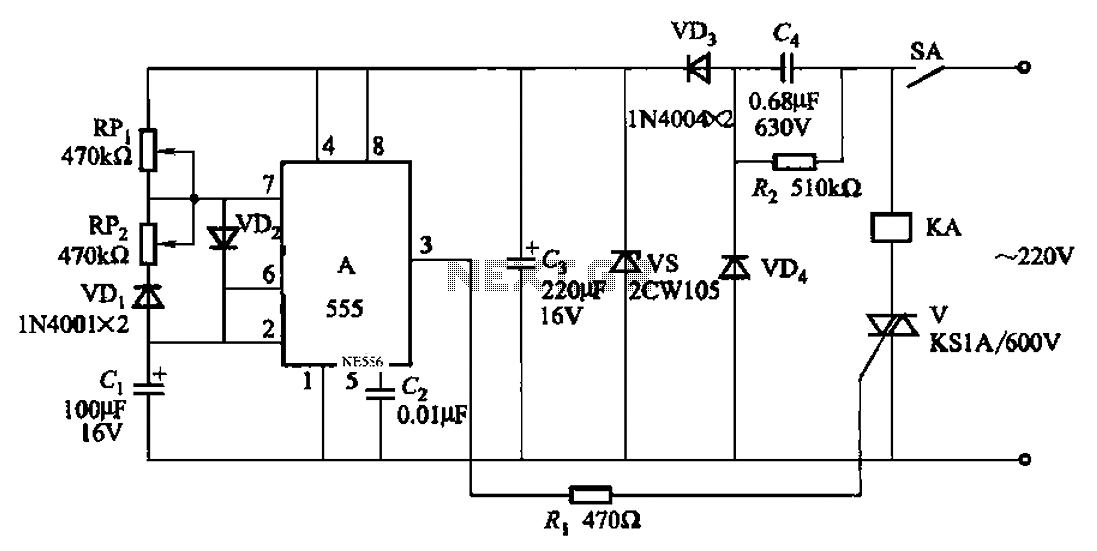
An automatic cycle switch circuit utilizing a 555 integrated circuit (IC) as the control element. It incorporates a capacitive step-down circuit and employs a bidirectional thyristor to control relays or loads with specific on and off timing. The circuit...
There are instances when a radio station can be found, and other times when no stations are detectable. The primary issue while tuning appears to be that any movement of the hands or body, such as releasing the tuning...