
Analog multiplexer CD4051 extension circuit 1
The CD4051 multiplexer is designed to facilitate the routing of multiple signals to a single output, making it highly useful in applications where signal management is critical. The device operates by allowing one of eight input signals to be selected and passed to the output based on the binary values present at the select inputs A, B, and C. The inhibit input (INH) provides additional control, allowing for the disabling of the selected channel when necessary.
In a multi-chip configuration, the proper management of the control signals is essential to ensure that only one multiplexer is active at any given time, thus preventing signal interference. This is achieved by using a combination of logic gates, such as inverters, to manage the enable states of each multiplexer. The design allows for scalability, enabling the user to expand the number of channels by simply adding more CD4051 devices and correctly configuring the address lines.
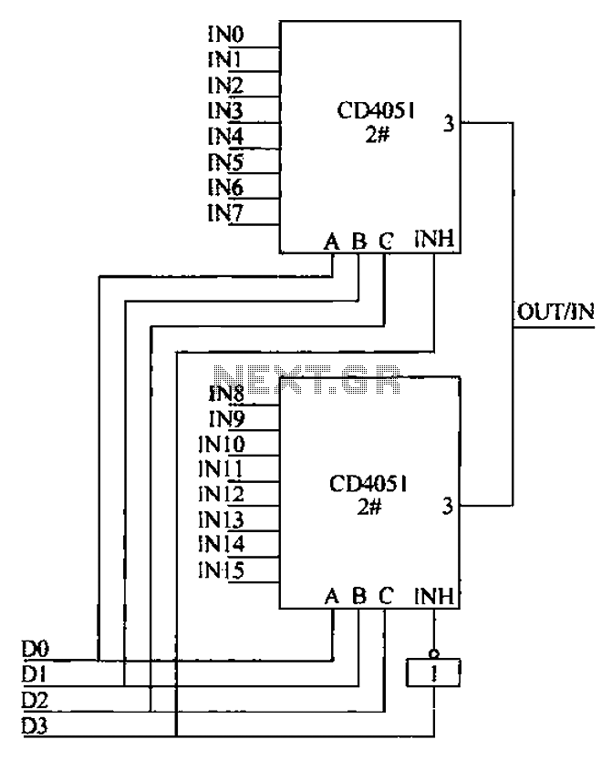
The integration of multiple CD4051 devices in a single system can be particularly advantageous in complex measurement and control applications, such as data acquisition systems, automated testing setups, and communication systems, where a large number of signals need to be multiplexed efficiently. The careful arrangement of the select lines and the inhibit input ensures that the system remains responsive and reliable, providing a robust solution for channel selection in electronic circuits. CD4051 is a single-ended input 8-channel multiplexer, it comes with three-pass channel select inputs A, B, C, and an inhibit input INH, input terminals A, B, C signal is used t o control the selection of eight channels It is turned on. In practice, if more than 8 measured parameters, using ten CD4051 multiplexer does not meet the requirements of large ones, which can be more than CD4051 connected and extended. Fig. 27-6 is composed of two CD4051 16 -channel multiplexer connection diagram. When multi-chip l switch-on work, multiplexer chip 2 on all off; on the contrary, the chip multiplex 2 opening when switched off, then the multi-switch chip 1 on all disconnected.
So, as long as a address (or data) line as the chip 1 and the chip 2 to allow control system side selection signal, and the two chip select input channels share a group address (or data) line. By changing the channel select lines D3 ~ DO status can gating one of the 16 channels INO ~ IN15. D3 is used to control the chip 1 and the core chip level INH input terminal 2. When D3-0 at which the chip l is fed in, in this context, DZ-DO terminal status is changed, only the strobe INO ~ IN7 one.
When D3-1 time, via the inverter goes low, the chip 2 is selected, this time, D2--; DO these three state lines, make the corresponding channel IN8-IN15 being turned on.
Related Circuits
The circuit diagram of an IC Controlled Emergency Light with Charger, also known as a 12V to 220V AC inverter circuit, is presented here. This circuit features automatic activation of the light during mains failure and includes a battery...
Low-noise preamplifier circuit. This circuit demonstrates a typical low-noise preamplifier design, which can be utilized to amplify signals from sources such as magnetic heads and microphones within audio applications. The input signal is coupled through a capacitor and subsequently...
This circuit was designed to transmit commands over an LNB coaxial cable. An LNB (Low-Noise Block downconverter) is commonly used for satellite TV reception and is positioned at the focal point of a satellite dish. The circuit generates a...

This document outlines the design process of a control circuit for a stepper motor. Given the characteristics of the stepper motor, the control circuit was developed as a state machine that transitions through four output states depending on two...
The applet shows a simulation of Chua's circuit, plotting the voltage measured across C1 against the voltage measured across C2. This corresponds to the display on an X-Y oscilloscope with probes connected across these capacitors. The initial values of...
This is a simple power resumption alarm circuit that can be installed within the switch box. It emits beeping sounds when power is restored following a power outage. The power resumption alarm circuit serves as a practical solution for alerting...