
Speech compression circuit diagram
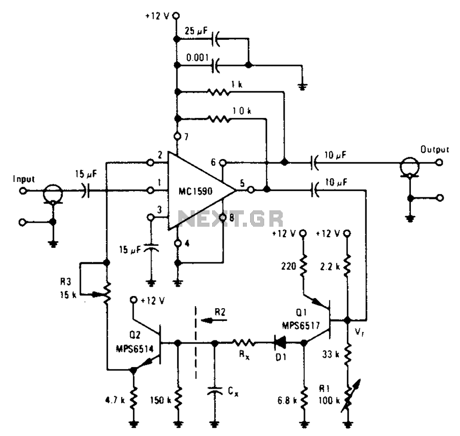
The amplifier circuit operates by leveraging the characteristics of the MPS6517 PNP transistor in an emitter follower configuration, which provides a high input impedance and low output impedance, making it suitable for driving loads. The voltage gain of approximately 20 indicates that the output voltage is 20 times the input voltage, allowing for significant amplification of weak signals.
The RI controller plays a crucial role in setting the static operating point of the transistor, ensuring optimal performance. By adjusting the quiescent point, the circuit can accommodate varying signal levels and maintain linearity in amplification. The reference voltage Vr, set at 7.0V, serves as a threshold that must be surpassed for the diode D1 to conduct. This feature prevents the amplifier from responding to noise or low-level signals, thus enhancing the signal-to-noise ratio.
When the input signal's peak exceeds the reference voltage Vr, diode D1 becomes forward-biased and conducts, allowing the positive peaks of the signal to pass through. This rectification process is essential for converting the AC signal into a usable DC output. The subsequent filtering stage, which includes capacitor Cx and resistor Rx, smooths the output signal, removing unwanted fluctuations and providing a stable voltage level.
The resistor Rx is particularly important as it determines the charging and discharging time constants for capacitor Cx. A larger resistance value will result in a longer time constant, leading to slower charging and discharging of the capacitor, which can be beneficial for applications requiring a gradual response. Conversely, a smaller resistance value will lead to a quicker response, making the circuit more reactive to changes in the input signal.
In summary, this amplifier circuit effectively manages signal amplification and processing through careful design considerations, including the choice of transistor, the implementation of a quiescent point adjustment mechanism, and the incorporation of rectifying and filtering components. These elements work together to ensure reliable performance in various electronic applications.Amplifier capable of driving a voltage gain of about 20 MPS6517 PNP type emitter electrode group is. RI controller can change the static point of the transistor Q, which is to change the quantity exceeds the signal level Vr. Only when the peak is greater than Vr when (Vr F7.0V), the output of the diode D1 can be rectified positive peaks Q1. The resulting output filters Cx and Rx. Rx control the charging time constant or time out. Charging and discharging are required to use Cx.
Related Circuits
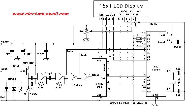
Frequency meter circuit for service applications, including all standard frequency bands: amateur HF, VHF, and UHF, displayed on an LCD screen. The frequency meter circuit is designed to accurately measure and display frequency across various amateur radio bands, specifically HF...
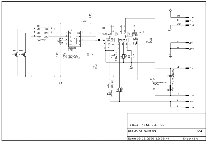
The following circuit illustrates a 2500W Phase Control Circuit Schematic. Features include a ground-tied trigger output that is disabled, and a low voltage input. The 2500W Phase Control Circuit is designed to regulate the power delivered to a load by...
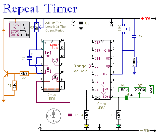
The CMOS 4060 integrated circuit (IC) features two built-in inverters located at pins 9, 10, and 11, which must be interconnected to create an oscillator. The output of this oscillator is available at Pin 9, which continuously alternates between...
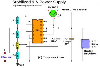
C1 filters the noise and spikes from the AC supply. The circuit can be adjusted to provide a 9V or 12V output voltage, or any other voltage level required by the PC mini drill, using the P1 potentiometer. The circuit...
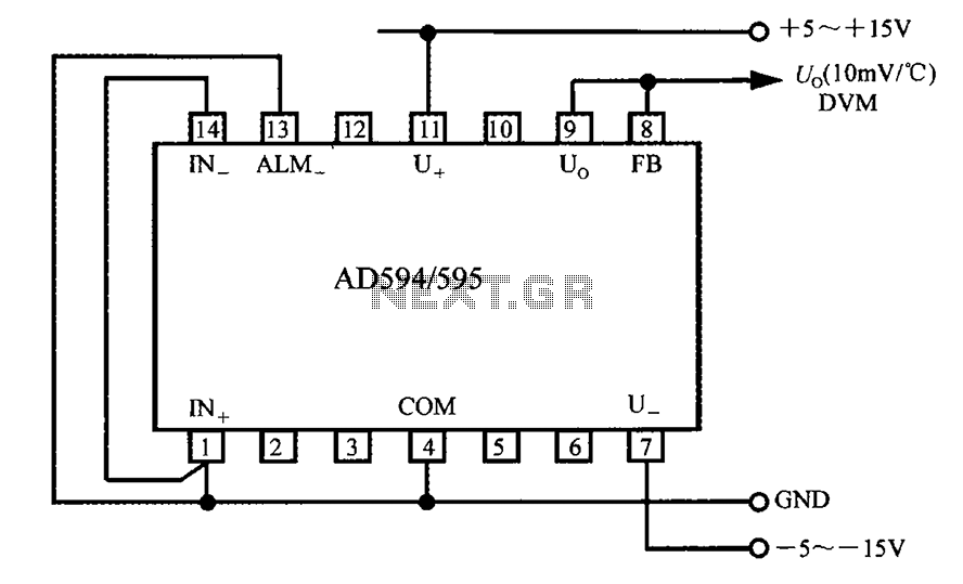
The AD594/595 can be configured to measure temperature in Celsius. In the circuit diagram, the IN+ and IN- terminals should be shorted to the COM terminal. The output voltage (Uo) has a temperature coefficient of 10 mV/°C, which can...
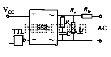
This document discusses the AC solid-state relay (AC-SSR) and presents its basic application circuit as illustrated in Figure (a). Additionally, it includes a TTL drive SSR circuit depicted in Figure (b), a CMOS driver circuit for the SSR shown...