
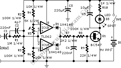
PCM1794A audio DAC
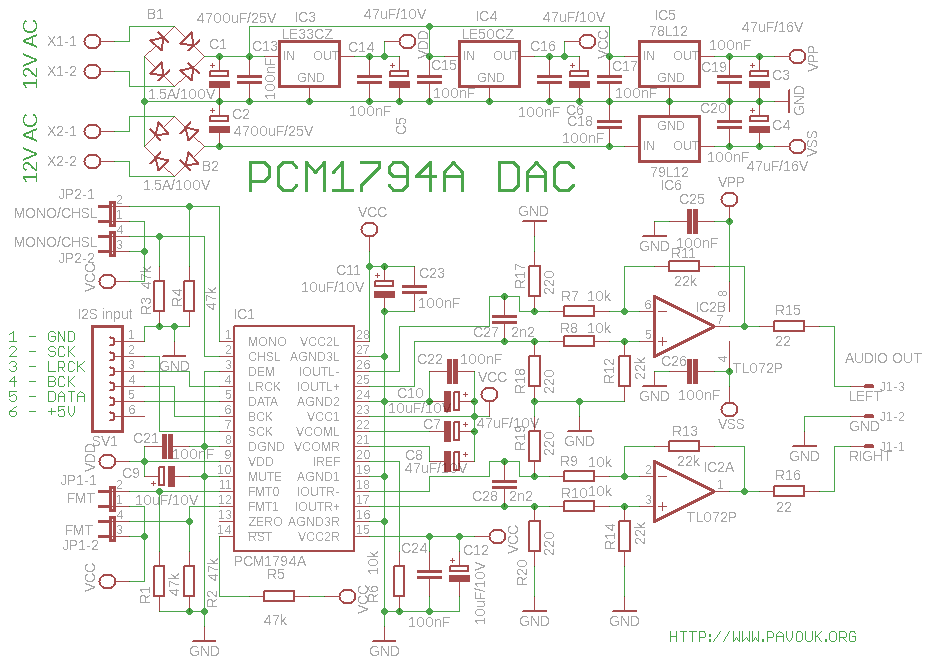
A comprehensive electronic schematic for the described circuit would include the following components and connections:
1. **Transformer**: A dual 12V secondary winding transformer, ensuring isolation and proper voltage levels for the DAC and decoder.
2. **Rectification**: Two bridge rectifiers (B1 and B2) to convert AC voltage from the transformer to DC voltage, followed by smoothing capacitors to reduce ripple.
3. **Voltage Regulation**: Low-dropout regulators (IC3 and IC4) to provide stable voltage levels for the analog and digital sections of the DAC.
4. **Operational Amplifiers**: IC5 and IC6 for generating +12V and -12V supplies for the operational amplifier circuitry.
5. **DAC (PCM1794A)**: Central component for digital-to-analog conversion, fed by an I2S bus with proper clocking from the SCK signal.
6. **Resistors**: High-quality carbon resistors (R17 to R20) for current-to-voltage conversion, arranged to ensure minimal signal degradation.
7. **Decoupling Capacitors**: Strategically placed close to the DAC to filter out high-frequency noise and stabilize voltage levels.
8. **Jumpers**: Configurable connections allowing for selection of audio format and system clock settings, ensuring compatibility with various data formats.
9. **PCB Design**: A single-sided layout with careful routing to minimize interference between digital and analog sections, featuring ground planes for stability.
10. **Reset Circuit**: Incorporating a pull-up resistor (R5) to ensure reliable operation of the reset function.
This schematic would provide a clear representation of the circuit's functionality and layout, ensuring optimal performance and ease of assembly for users.For power supply is needed transformer with two individual secondary 12V windings. If you want to supply from transformer S/PDIF decoder and transformer doesn`t have third separated winding, we must connect supply input of decoder parallel to winding for positive branch otherwise there will be short circuit. Voltage is rectified by B1 and B2 bridg es and goes through filter and decoupling capacitors to low-drop regulators IC3 and IC4 which feeds analog and digital part of DAC. IC5 and IC6 regulates voltage +12V and -12V for operational amplifier. All supply inputs of DAC are properly decoupled with capacitors. DAC PCM1794A works with data from standard I2S bus. In addition to it use signal SCK - System clock, which needs for proper function and oversampling. Input data format, output type and characterics of digital filter is selected with jumpers. Circuit includes internal reset with external pull-up resistor R5. Output is current differential. For conversion to voltage output I use resistors R17 to R20. They should be high quality carbon resistors. Behind these resistors we can theoretically take out symmetrical output to high impedance input of preamplifier.
C27 and C28 are used for limit of high frequencies out of audible sound. For getting of single-ended output with average value at zero I used low-noise operating amplifier TL072. Gain is about two. I inspired by original circuit because I am not specialist for operating amplifiers. In original circuit are used operating amplifiers for conversion of current to voltage output too. I used only resistors which are better and simpler. In quiet outputs have zero voltage, that theoretically we don`t need coupling capacitors. On one output was voltage about 12mV and on another 2. 6mV. It can be better by selecting value of resistors. Parts are placed from smaller to bigger. I begin with IC1. Method of his placing is same like on S/PDIF decoder. Next I continued with SMD resistors and capacitors. Next I placed wire connections and components from a top side of board and last connectors. Printed circuit board is single sided with two wire connections, that it can be easily made in amateur conditions.
Ground wires are drawed with accent to separating of digital and analog part. Decoupling capacitors are placed closely to DAC. PCB of prototype on photos is a little different in these smallness: In schematics is additional pull-up resistor R5 on a reset signal. In datasheet is not discoverable that it must be used. SMD resistors and capacitors with size 0805 was replaced with 1206 size for easier mounting. I was succesful in reducing of wire connections from five to two. Circuit is configured with 4 jumpers. When they are not installed, that they are pull-downed to zero with resistors. Setting of audio format is described next in the table. Most frequently I meet with I2S or right-justified 24bit format. If we connect board to our S/PDIF decoder, we must on them set identical data format and frequency of system clock.
If we want to play 192kHz samples, we must set system clock maximally to 384 x fs. More informations are in a datasheet. Audio DAC with PCM1794A has excellent parameters and sounds great. Traces on a scope looks very good too, but with high frequency 20kHz with sample frequency 44. 1kHz we can see in a trace instead of "stairs" some smoothed connection with multiple traces. It is probably normal in a DAC with oversampling. My goal is to have DAC without oversampling which should guarantee high fidelity of playing. Circuit doesn`t worked immediately for me. Reason was missing pull-up resistor on RESET signal. It could have insufficient description of reset function and incomplete schematics of circuit in a datasheet or my misunderstanding. For getting better parameters it is possible to try change operational amplifier TL072 with something better.
We can completely bypass output amplifier and use symmetrical 🔗 External reference
Related Circuits
This audio meter can be monitored using a small panel meter with a circuit constructed from discrete components. The audio level meter circuit exhibits a flat frequency response ranging from approximately 20Hz to over 50kHz. The input sensitivity is...
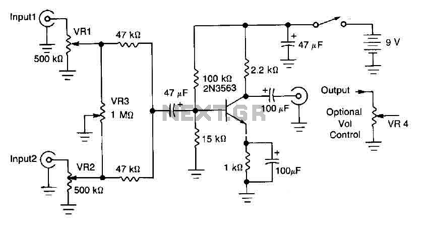
This circuit mixer features internal amplification using a 2N3563 transistor. Two input signals can be independently adjusted via VRI and VR2. The VR3 balance control allows for the attenuation of one signal while the other remains active. Additionally, the...
This weblog discusses electronic circuit schematics, PCB design, DIY kits, and electronic project diagrams. The subject circuit is a quality preamplifier with a built-in USB DAC designed for the Leachamp power amplifier. The schematic is based on the PCM2902...
A window comparator formed by two operational amplifiers packaged into IC1 is the heart of the circuit below. With this technique, we can detect precisely and symmetrically. The window comparator circuit utilizes two operational amplifiers (op-amps) configured to create a...
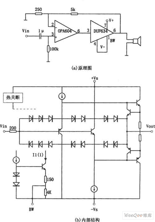
The provided image depicts a high-performance and low-power audio power amplifier circuit. The initial stage utilizes the MOSFET hi-fi operational amplifier OPA604, while the subsequent stage employs the high-speed buffer BUF634. Voltage series negative feedback is implemented between the...
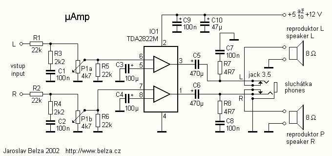
The amplifier is based on an integrated circuit TDA2822M. With this circuit, an amplifier can be built with up to 2 W. This much power circuit is able to supply only at peak times; continuous excitation would not be...