
PCM2706 USB DAC with I2S
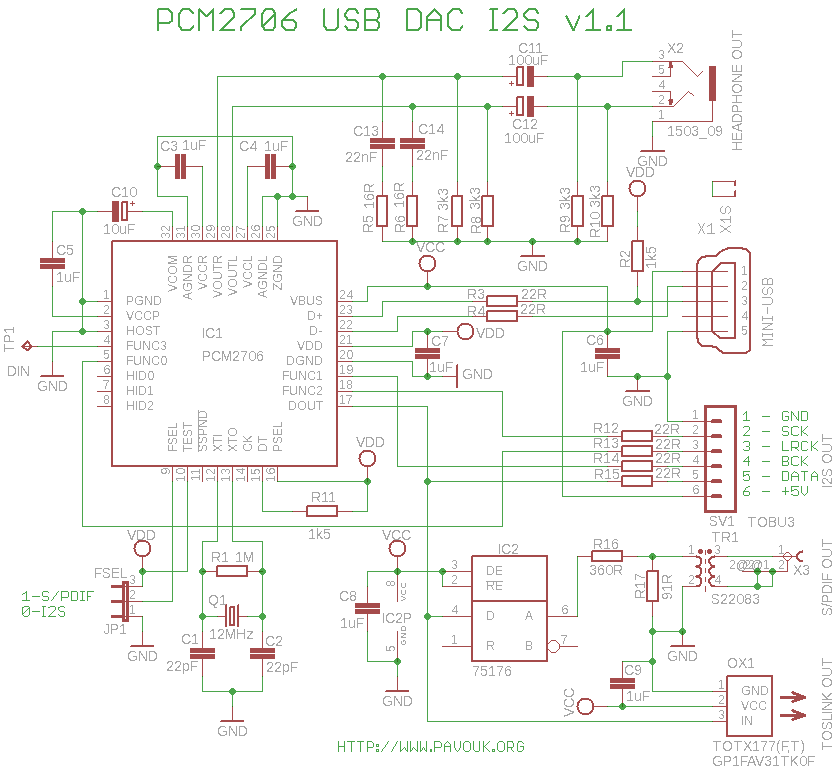
The circuit design centers around the PCM2706, which integrates a USB interface, a DAC, and an S/PDIF output. The digital volume control feature enhances user experience by allowing precise adjustment of sound levels through the analog output, while ensuring that the digital outputs remain unaffected. The galvanic isolation of the S/PDIF output is critical in preventing ground loops and ensuring signal integrity, especially when interfacing with other audio equipment.
The PCB layout emphasizes ease of assembly and flexibility. The decision to place SMD components on the bottom side while leaving the top side for wire wraps and connectors is strategic, allowing for easier soldering and maintenance. The modular approach to component assembly ensures that users can customize the board according to their specific needs, omitting unnecessary parts based on the desired functionality.
The inclusion of both S/PDIF and I2S outputs caters to a wide range of audio applications, from basic headphone amplification to more complex setups involving external DSPs. The careful consideration of signal paths, isolation, and component placement demonstrates a thorough understanding of audio circuit design principles, ensuring a reliable and high-quality audio output.A couple of USB DACs but no one have I2S output. Some people doesn`t need S/PDIF input and they want only USB. With these requirements is unnecessary to convert signal first from USB to S/PDIF and next to I2S for DAC. This board have analog headphone output, electric galvanically isolated S/PDIF output and optical TOSLINK.
After switching jumper circuit switch to I2S mode, which can be directly connected to DAC. Diagram use PCM2706 circuit from Texas Instruments. Circuit includes Digital/Analog converter, S/PDIF output, I2S output and HID interface for push buttons. Schematics diagram is similar to recommended diagram in datasheet. USB input has standard miniUSB connector. Circuit PCM2706 has integrated headphone amplifier and his output goes through external low-pass filter to standard 3.
5" jack socket. Circuit includes digital volume control in a range 0dB to -64dB with 1dB step. This control works only with analog output. It doesn`t have effect for I2S and S/PDIF outputs. In S/PDIF mode (FSEL=1) is active S/PDIF data output and on pins FUNC0 to FUNC3 are inputs for push buttons, which are not used. S/PDIF output goes to optical transmitter and to RS485 driver which boosts signal to voltage divider which divide signal approximately to 1 volt and adjust output impedance to about 75 ohms.
Signal is galvanically isolated by pulse transformer. In I2S mode (FSEL=0) goes to the DOUT data in I2S format (16 bits left justified) and on pins FUNC0 to FUNC2 are LRCK, BCK and SYSCK signals. On the pin FUNC3 is now I2S data input signal which is connected to the internal DAC. In my circuit is only on the testpoint and headphone output is silent in this mode. If you want to have active this output in I2S mode, that you can connect it with DOUT. This functionality is described for use with sound effects with external DSP. I2S output is not isolated that if you want them galvanically isolate you must use external isolator.
Schematics should work with PCM2707 circuit too, because I keeped all connection requirements for both chips. This was not tested because I hadn`t this chip available. We place components on the board from smaller to bigger. We begin with integrated circuits and next continue with other SMD components. Next we continue from a top side with wire wraps and other components. Last we assemble connectors. If you don`t want to use for example analog output, that you don`t need assemble parts of analog filter and jack connector.
If you don`t want electrical S/PDIF output that don`t assemble IC2, R16, R17, TR1 and X3. Optical output includes only C9 and OX1. Printed circuit board is single-sided which allows to create him in amateur conditions. SMD components are from a bottom side and parts with wires, wire wraps and connectors from a top side. Board dimensions was changed a little in a 1. 1 version for direct connection with DAC boards. It allows to have connectors on a back panel with boards in one line. 🔗 External reference
Related Circuits

Problems can arise with USB hubs powered from a PC when devices connected to them draw excessive current. This situation often occurs with devices that use USB cables that are either too long or too thin, leading to voltage...
An increasing number of devices operate on internal rechargeable batteries. While a compatible charger is typically included, some devices can only be charged via a USB port. This is common with USB MP3 players, which require docking with a...
The enable signal for the USB chip and GLCD controller is generated by a PLD decoder from the address lines. The memory map for the I/O of the 8051SBC board indicates that the available space ranges from 0x0300 to...

With a DPDT switch, I can switch the two data lines. I tried connecting the shields from the two computers together, the grounds two computers together, switching the D+ and D- lines with the DPDT switch, and leaving the...
In the past, it was straightforward to utilize the parallel port of a standard PC to program various types of AVR microcontrollers. Currently, one must purchase a programmer that connects to the PC via USB, which increases the complexity...
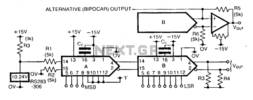
The step size of the converter is variable by selecting the high-order data bits. The first DAC, A, has a stable reference current supplied via a 10.24 V reference IC and resistor R1. Resistor R2 provides bias cancellation. Only...