
peak detector

The circuit operates by utilizing two operational amplifiers, U1 and U2, configured as voltage followers to ensure that the output voltage closely follows the input voltage without loading the circuit. The input voltage, applied at Vj, is directed to capacitor C1 through diode D1. The diode allows current to flow in one direction, ensuring that C1 charges to the peak voltage level of the input signal. This configuration is essential for maintaining the peak voltage on C1, which is crucial for applications requiring peak detection.
Capacitor C1 must be chosen carefully to minimize leakage current and dielectric absorption, which can affect the accuracy of the peak voltage held. Low leakage ensures that the capacitor does not discharge significantly over time, while low dielectric absorption prevents the capacitor from retaining unwanted charge, which could lead to erroneous readings.
The reset functionality is an important aspect of this circuit. It allows the stored peak voltage to be cleared either manually or electronically. A manual reset can be implemented using a switch that short-circuits C1, discharging it completely. Alternatively, an electronic reset can be achieved using a field-effect transistor (FET) that is normally off. When triggered, the FET will conduct, effectively discharging C1 and allowing for a new peak voltage to be captured.
To detect negative peak values, diode D1 can be reversed, allowing negative voltages to charge C1. This flexibility enhances the circuit's utility in applications where both positive and negative peak detection is necessary.
Overall, this circuit provides a reliable means of capturing and holding peak voltages, with considerations for reset mechanisms and component selection critical to its performance.The purpose of the circuit is to hold the peak of the input voltage on capacitor Cl, and read the value, V0, at the output of U2. Op amps Ul and U2 are connected as voltage followers. When a signal is applied to Vj, Cl will charge to this same voltage through diode Dl. This positive peak voltage on Cl will maintain V0 at this level until the capacitor is reset (shorted).
Of course, higher positive peaks will raise this level while lower power peaks will be ignored. Cl can be reset manually with a switch, or electronically with an FET that is normally off. The capacitor specified for Cl should have low leakage and low dielectric absorption. Diode Dl should also have low leakage. Peak values of negative polarity signals may be detected by reversing Dl.
Related Circuits
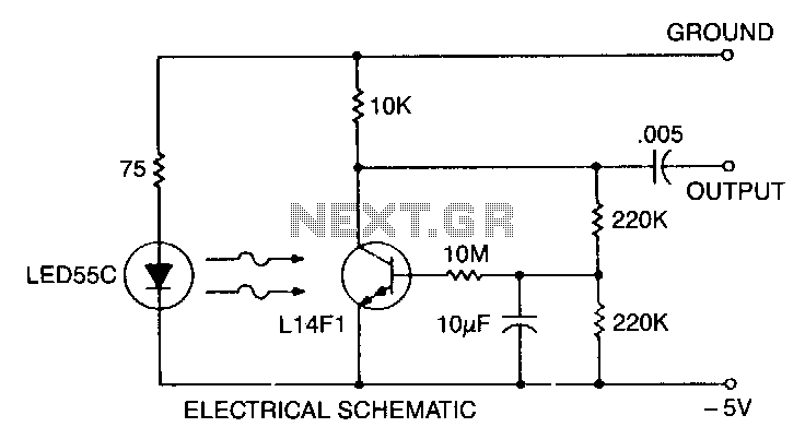
This self-biasing configuration is useful whenever small changes in light level must be detected, such as when monitoring very low flow rates by counting drops of fluid. In this bias method, the photodarlington is bias stabilized by feedback from...
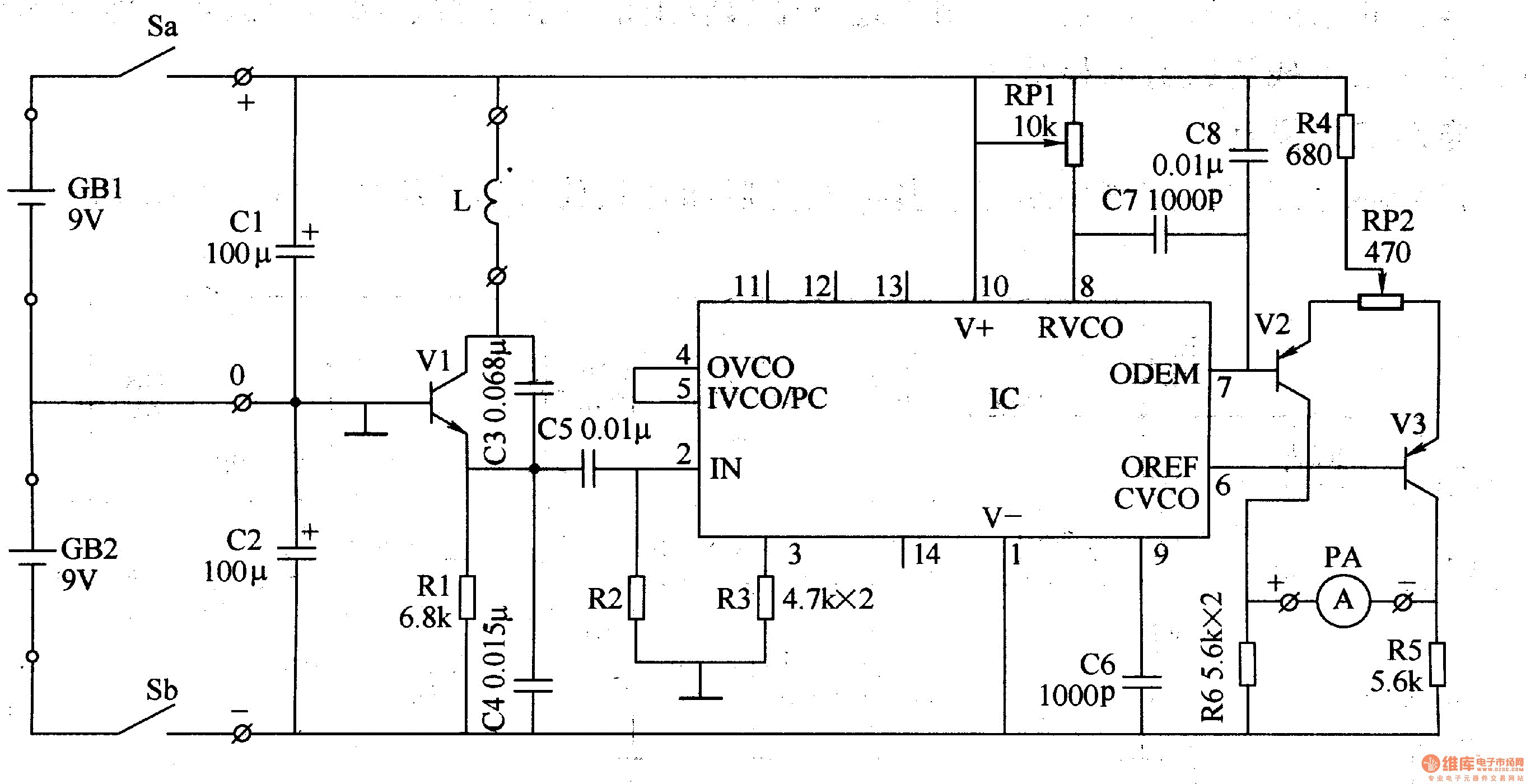
The metal detector described in the example can detect metal objects made of highly permeable magnetic substances. The circuit operates based on several components: a power circuit, a sine wave oscillator, a PLL (phase-locked loop) circuit, and a hybrid...
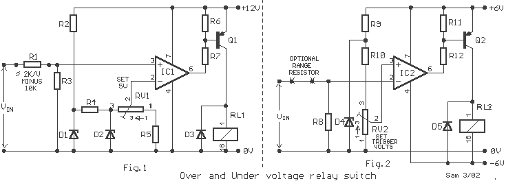
In Fig. 1 A precision DC undervoltage relay switch. The op-amp is wired as a voltage comparator, with a reference voltage applied to pin 2 and the test voltage applied to pin 3: the relay turns on when the...
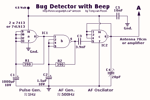
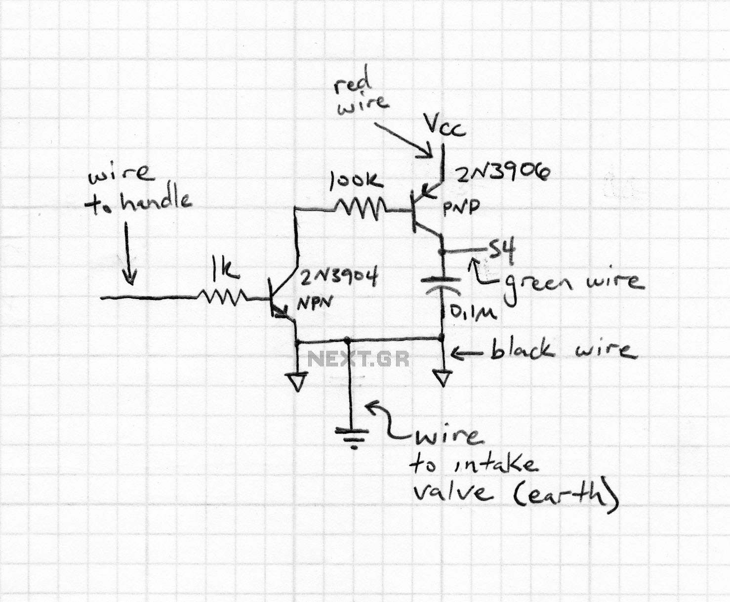
This circuit is not open for discussion. Although working perfectly, it was experimental. I will answer no emails in regards to this circuit. If you are looking for a more serious and reliable bug detector, go to the Countersurveillance...
The GLMDPCB motion detector board is a double-sided etched, screened, and drilled printed circuit board designed for the GLMDA motion detector circuit illustrated in the schematic below. The circuit can be constructed in its entirety or in part. For...
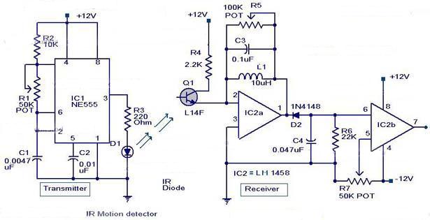
The circuit diagram depicts an infrared motion detector designed to detect intrusions. Infrared rays reflected from a stationary object exhibit one phase, while rays reflected from a moving object display a different phase. This principle is utilized for motion...