
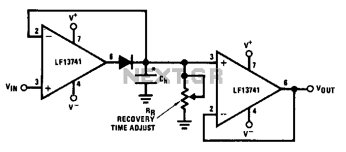
Phase detector with 10-bit accuracy
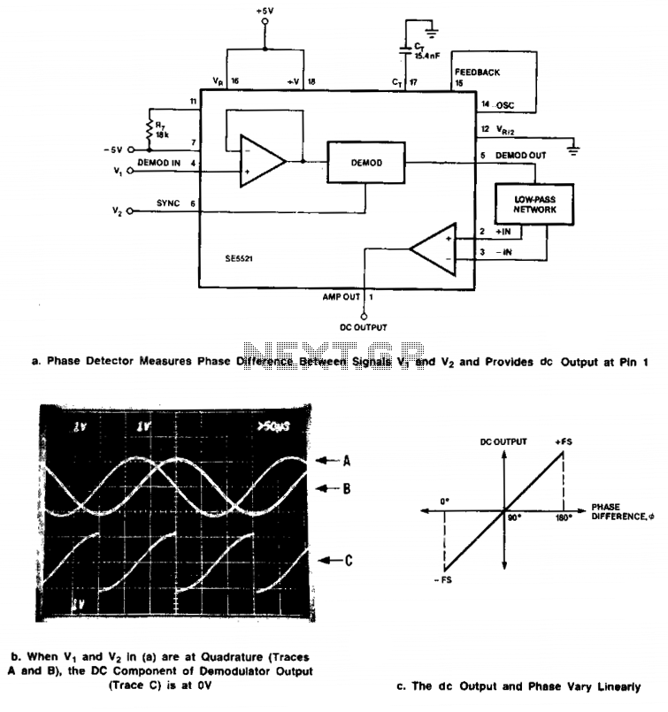
The circuit described utilizes a phase detector configuration that is effective in applications requiring precise phase comparison between two signals of identical frequency. The demodulator's sync input (Pin 6) and demodulator input (Pin 4) are designed to accept signals that are synchronized in frequency, allowing for accurate detection of phase differences. The output DC voltage from the demodulator is directly related to the phase relationship of the input signals, providing a clear indication of whether the signals are in phase or out of phase.
For dual supply operation, the reference point is set to 0 V, ensuring that the signals remain within the operational limits of the demodulator. In single supply operation, the reference voltage is adjusted to VR/2, which effectively centers the input signals around a mid-scale point, allowing for optimal performance. The design accommodates ±5 V supply voltages, enabling the demodulator to process input signals with a peak-to-peak voltage of 7 V, making it suitable for a variety of signal types.
The low-pass filter network, connected to the uncommitted amplifier output at Pin 1, plays a crucial role in smoothing the output signal. This configuration helps to eliminate high-frequency noise and provides a cleaner DC output that accurately reflects the phase difference between the input signals. The behavior of the output is significant: the maximum output occurs when the two input signals are 180° out of phase, indicating a full-scale positive output, while a minimum output is produced when the signals are perfectly in phase, resulting in a full-scale negative output. This functionality is essential for applications such as phase-locked loops, frequency modulation demodulation, and other systems where phase information is critical.Signals of identical frequency are applied to sync input (Pin 6) and to the demodulator input (Pin 4), respectively, the demodulator functions as a phase detector with output dc component being proportional to phase difference between the two inputs. The signals must be referenced to 0 V for dual supply operation or to VR/2 for single supply operation.
At ± 5-V supplies, the demodulator can easily handle 7-V peak-to-peak signals. The low-pass network configured with the uncommitted amplifier dc output at Pin 1 of the device. The dc output is maximum (+ full-scale) when Vj and V2 are 180° out of phase and minimum (- full-scale) when the signals are in phase. 🔗 External reference
Related Circuits
An accurate phase shift of 90 degrees can be achieved using a variable resistor (VR) and an operational amplifier (op-amp). The adjustment allows for a specific frequency to be manipulated. The phase shift can range from 180 degrees to...
The DIAC, or diode for alternating current, is a trigger diode that conducts current only after its breakdown voltage has been momentarily exceeded. Most DIACs are utilized in applications requiring a switching function in AC circuits. The DIAC is a...
This electronic liquid detector circuit diagram is based on the ULN2429 monolithic bipolar integrated circuit designed for detecting the absence or presence of many different types of liquids. The ULN2429 electronic liquid detector circuit can be used in automotive,...

This circuit monitors the duration of an incoming pulse. If the incoming pulse is shorter than the set value (VAR1), the output of U1B remains high. Values are provided for a 1 to 2 microsecond pulse. The described circuit functions...
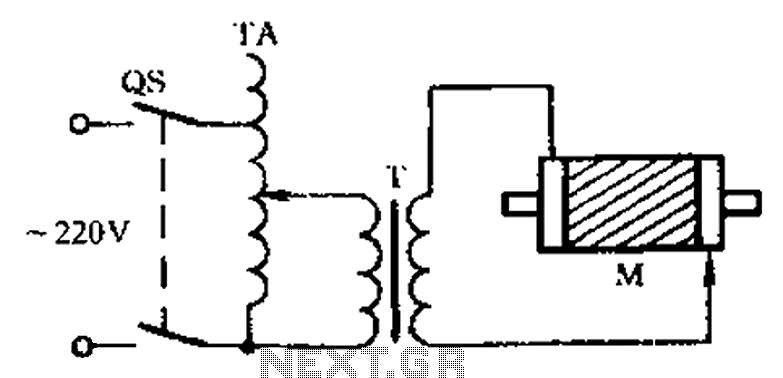
The circuit diagram illustrates a three-phase motor equipped with an inspection circuit designed to detect broken bars. The circuit for a three-phase motor with a broken bar inspection system typically consists of several key components that work together to monitor...
This circuit utilizes operational amplifier U1 to correct the offset in the peak detector diode D1. The voltage across capacitor C is the precise peak voltage. Additionally, U2 functions as a voltage follower to measure this voltage. The described circuit...
Warning: include(partials/cookie-banner.php): Failed to open stream: Permission denied in /var/www/html/nextgr/view-circuit.php on line 713
Warning: include(): Failed opening 'partials/cookie-banner.php' for inclusion (include_path='.:/usr/share/php') in /var/www/html/nextgr/view-circuit.php on line 713