
Photocell Amplifier
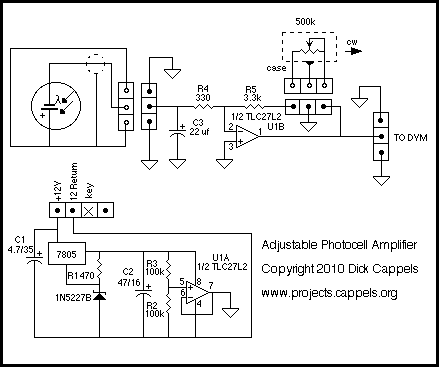
Starting with the power supply. An input voltage of 12 to 16 volts DC is regulated to +8 volts. R1 assures that a minimum of 10 milliamps flows through the 1N5227, 3.6-volt Zener diode. All together, this makes approximately 8.6 volts. This would have been simpler with a 7808 regulator, and a low power version of the regulator would have been plenty sufficient, but one works with what one has on hand.
The 8 volts is split by R2 and R3 to produce a ground reference voltage at half the regulated supply voltage. This results in power to the op-amp of +4 volts and -4 volts. Very little current flows between the power positive and negative rails, so U1A, which provides a low impedance ground reference, is not really needed, but the op-amps came two to a package, and not having to pay much attention to the effects of power supply current returning through the ground made life a little simpler, so I went ahead and used U1A in this role.
The photocell is connected to the amplifier through approximately two meters of Belden RG-174/U miniature coax cable. All that is desired is to measure the average current, so the current from the photocell is filtered by C3 to reduce the amount of hum and other modulation of the current. The capacitor, along with R4, forms a 20 Hz single-pole low-pass filter, which after examination of the output on a scope, is adequate for the needs.
The actual amplification is done by the TLC2712 op-amp. Feedback from the output to the inverting input through 3.3k R5 and the 500k pot allows transimpedances from very low 3.3 k ohms to 500 k ohms. R4 is to limit noise gain while R5 limits the closed-loop gain, thereby assuring that some loop gain remains and that the amplifier remains stable.
The circuit operates with a regulated voltage supply, maintaining a stable output for accurate measurements. The choice of the TLC2712 op-amp is significant due to its low noise characteristics, which are essential for precision applications involving photodiodes. The feedback network, consisting of R5 and the variable resistor (potentiometer), allows for fine-tuning of the gain, accommodating various input levels from the photodiode.
The low input resistance of the amplifier is crucial for ensuring minimal loading on the photocell, allowing it to operate in a near-zero bias condition. This configuration is intended to maximize the linear response of the photocell to incident light, ensuring that variations in light intensity translate directly to variations in output voltage.
The layout of the connectors at the bottom of the board facilitates easy integration with external measurement devices, such as digital voltmeters, and provides flexibility in using different types of photodiodes. The choice of coaxial cable for connecting the photocell helps in minimizing interference and maintaining signal integrity over the two-meter distance.
Overall, the design emphasizes stability, noise reduction, and accurate measurement capabilities, making it suitable for applications in light sensing and photometry.The output of the amplifier is to be measured on a digital voltmeter. Besides being able to accept 20 na to 200 micro amps and output voltages that range form 100 mv to 2 or 3 volts, the amplifier needed to have a low input resistance so the diode could be run at or near zero bias so that its output would be a linear function of light on the photocell. It also has to have plenty of connectors. Along the bottom of the board in the image above, from left to right, are a power input connector because it would use an isolated unregulated DC power supply that is sometimes used for other things, a voltage output connector so that its output could be plugged into a digital voltmeter, and an input connector so that it can accept current from a variety of photodiodes.
Starting with the power supply. An input voltage of 12 to 16 volts DC is regulated to + 8 volts. R1 assures that a minimum of 10 milliamps flows through the 1N5227, 3.6 volt Zener diode. All together, this makes approximately 8.6 volts. This would have been simpler with a 7808 regulator, and a low power version of the regulator would have been plenty sufficient, but one works with what one has on hand. The 8 volts is split by R2 and R3 to produce a ground reference voltage at half the regulated supply voltage.
This results in power to the opamp of +4 volts and -4 volts. Very little current flows between the power positive and negative rails, so U1A, which provides a low impedance ground reference, is not really needed, but the opamps came two to a package, and not having to pay much attention to the effects power supply current returning through the ground made life a little simpler, so I went ahead and used U1A in this role. The photocell is connected to the amplifier through approximately two meters of Belden RG-174/U miniature coax cable.
All I want to measure is the average current so the current from the photocell is filtered by C3 to reduce the amount of hum and other modulation of the current. The capacitor, along with R4 form a 20 Hz low single pole low pass filter which after examination of the output on a scope, is adequate for my needs.
The actual amplification is done by the marvelous TLC27l2 opamp. Feedback from the output to the inverting input through 3.3k R5 and the 500k pot allows transimpedances from very low 3.3 k ohms to 500 k ohms. R4 is to limit noise gain while R5 limits the closed loop gain, thereby assuring that some loop gain remains and that the amplifier remains stable.
🔗 External reference
Related Circuits
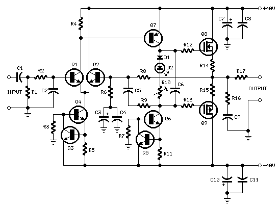
The power supply has been simplified. Power transformers and rectifiers have been omitted, and some components have been removed from the MOSFET voltage regulator circuits: 1N5242 zener diodes between the source and gate and 10k resistors in series with...
In specific applications, such as transmitters or other communications and control systems, this circuit is designed to be beneficial. It provides both audio output and DC control outputs. Additionally, R9 establishes the control threshold. The circuit in question is versatile...
This document serves as a compilation of design notes, providing practical details as construction progresses, along with some photographs that will be included in due course. Currently, it functions as a progress report, blending immediate plans with actual construction,...
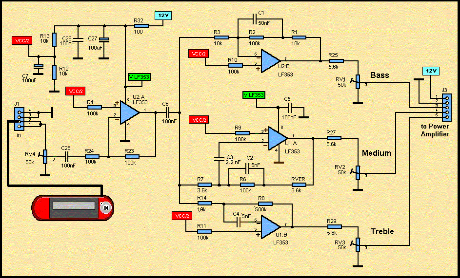
A diagram of an active loudspeaker. The LF353 from National Semiconductor will split the audio signal into three bands. The SANYO LA47536 will amplify these signals. In stereo mode, eight high speakers will create significant sound pressure. The LF353...
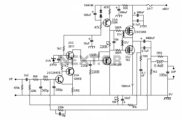
In this circuit we use the 2SK1058 and the 2SJ162 Mosfets. This could be avoided by a fairly simple bootstrapping circuit, but the improvement in maximum output may be just a fraction of a dB, depending on the supply...
R1_47K 1/4W Resistor, R2_4K7 1/4W Resistor, R3_22K 1/4W Resistor, R4_1K 1/4W Resistor, R5, R12, R13_330R 1/4W Resistors, R6_1K5 1/4W Resistor, R7_15K 1/4W Resistor, R8_33K 1/4W Resistor, R9_150K 1/4W Resistor, R10_500R 1/2W Trimmer Cermet, R11_39R 1/4W Resistor, R14, R15_R33 2.5W...