
Photoreceiving circuit diagram LM307 amplifier configuration

The photoelectric receiver amplifier circuit operates as a vital component in various optoelectronic applications, where accurate light intensity measurements are essential. The configuration typically consists of a photodiode or phototransistor connected to the non-inverting input of the LM307 op-amp. The output voltage (Vo) is monitored across a load resistor (R1), which converts the amplified photocurrent into a usable voltage signal.
The circuit's performance is influenced by several parameters, including the bias voltage (VB), which sets the operating point for the phototransistor. A negative bias, such as -15V, is commonly used to enhance the sensitivity and response time of the phototransistor. The LM307 op-amp is selected for its low input bias current and high gain characteristics, making it suitable for amplifying small signals generated by the photodetector.
In practice, the circuit can be fine-tuned by adjusting the value of R1 to achieve the desired sensitivity and output range. Additionally, the stability of the amplifier can be enhanced by incorporating feedback components that mitigate noise and improve linearity. The overall design ensures that the circuit can effectively respond to varying light conditions, making it applicable in fields such as optical communication, sensor technology, and automated lighting systems. As shown for the photoelectric receiver amplifier. Photo receiver amplifier for amplifying circuit amplifies the electrical signal photodiode or phototransistor optoelectronic device output and design. When the illuminance of the incident light changes, the photosensitive device will produce a corresponding voltage or current, and the photoreceptor amplifier is used to amplify the photocurrent change circuit constituted by the operational amplifier LM307 current amplifier it is ideally suited to achieve the above effect. In phototransistor OS18 with a certain bias voltage VB (FIG. (A) in VB -l5V), in the light of its output current operational amplifiers amplified output voltage Vo IpR1 to represent.
Minimum photocurrent Ip is determined by the LM307 op amp input bias current IB, the maximum value Ip by op amp maximum allowable output voltage Vomax decision.
Related Circuits
Frequency converter schematic, frequency to voltage converter schematic, frequency to voltage converter using TR, voltage to frequency converter application. A frequency converter is an essential electronic circuit that transforms frequency signals into corresponding voltage levels or vice versa. The frequency...
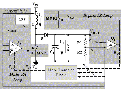
The main ΣΔ loop operates in steady state and is fully controlled by summing comparator Q2. This comparator amplifies the ripples of the sensed inductor current and output voltage with gains KI and KV, respectively, to generate an internal...
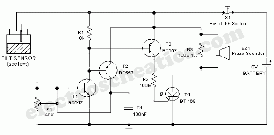
The ultra-simple tilt sensor alarm circuit can be constructed using readily available, inexpensive components. This circuit is based entirely on transistor technology. The homemade tilt sensor consists of a small glass or plastic bottle with two metal needles inserted...
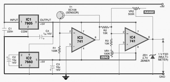
This DIY digital thermometer circuit can measure temperatures up to 150°C with an accuracy of ±1°C. The temperature is displayed on a 1V full scale deflection. The digital thermometer circuit is designed to provide accurate temperature readings within a specified...
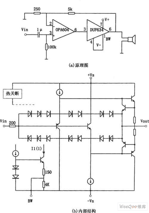
The provided image depicts a high-performance and low-power audio power amplifier circuit. The initial stage utilizes the MOSFET hi-fi operational amplifier OPA604, while the subsequent stage employs the high-speed buffer BUF634. Voltage series negative feedback is implemented between the...
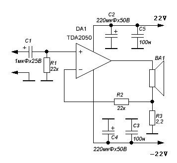
TDA2050 audio amplifier circuit diagram. The circuit incorporates environmental protection, where the output signal travels through connecting cables and the speaker’s network. In this case, the reactance of the circuit section connected to pin 4 of the chip is...