
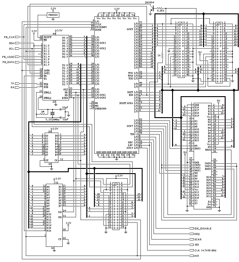
PJRC MP3 Player Schematic Diagrams
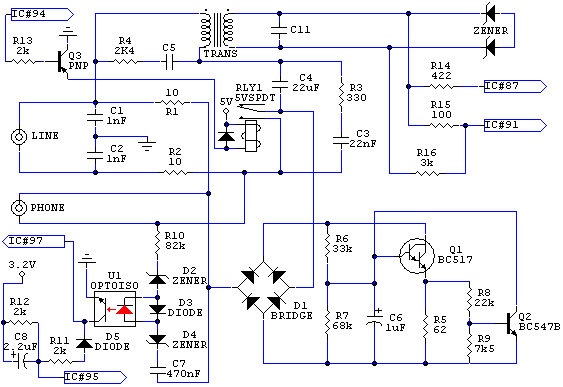
The circuit features a combination of polarized capacitors strategically placed to ensure optimal performance of the power supply system. Specifically, there are four 470 µF capacitors arranged in parallel, with two located above and to the right of the transformer. These capacitors are essential for maintaining low equivalent series resistance (Low-ESR) to enhance the efficiency of the power supply, particularly under varying load conditions. The selection of Low-ESR capacitors helps in minimizing voltage ripple and improving transient response, which is critical for stable operation.
Additionally, the circuit incorporates capacitors that were modified from 100 µF 16V to 33 µF, sourced from PJRC, which are also Low-ESR types. This change is aimed at further reducing noise in the power supply, thus enhancing the overall performance of the circuit. The use of standard capacitors ranging from 22 µF to 220 µF is permissible, providing flexibility in component selection while still maintaining functionality.
A notable component in the circuit is the 2.2 µF capacitor connected to pin 5. This component is crucial as it determines the time constant for the power supply's automatic shut-off feature. In scenarios where the output is shorted or the input voltage drops below a certain threshold, this capacitor ensures that the power supply responds appropriately by shutting down to prevent damage.
Moreover, the schematic includes diodes represented between the source and drain of two MOSFET transistors. It is important to note that these diode symbols correspond to the intrinsic diode structures found within the MOSFETs themselves, rather than indicating separate diode components that are physically mounted on the circuit board. This design choice simplifies the layout and reduces the number of discrete components, thereby optimizing space and potentially lowering costs in manufacturing.
In summary, the circuit design emphasizes the importance of component selection, particularly with respect to capacitor types and values, to ensure reliable and efficient power supply operation. The integration of Low-ESR capacitors, alongside careful consideration of timing components and internal diode structures, reflects a thoughtful approach to circuit design in electronic applications.The two unspecified polarized capacitors (one directly above the transformer and one directly to the right of the transformer) are actually each a pair of 470 µF capacitors in parallel (for a total of four 470 µF capacitors). These capacitors MUST be Low-ESR types for the power supply to function properly. Figure 4: The two 100 µF 16V capacitors were changed to 33 µF. PJRC provides these as Low-ESR capacitors to reduce noise. Standard capacitors, from 22 µF to 220 µF are likely to work. Figure 4: The 3. 3 µF capacitors attached to pin 5 should be 2. 2 µF (either value will work, but we have been using 2. 2 µF on the assembled boards and unassembled kits). This capacitor sets the time constant before the power supply will automatically shut off when the output is shorted or the input voltage is too low. Figure 4: The diodes shown connected between the source and drain on the two MOSFET transistors are the diode structures inside transistors.
These two diode symbols do not represent actual diode components soldered to the circuit board. 🔗 External reference
Related Circuits
This diagram illustrates the interaction between an internal SoftV92 Data Fax Modem and a phone line. The modem is manufactured by Zoltrix, although a Conexant utility identifies it as a "Churchill Data Modem." This schematic may be beneficial for...
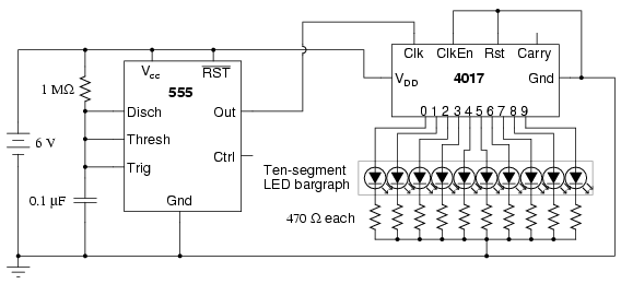
The following circuit illustrates a schematic diagram of an LED sequencer. This circuit is based on the 555 timer integrated circuit (IC). Features include a 555 timer circuit designed to debounce a mechanical switch, a 555 timer circuit to...
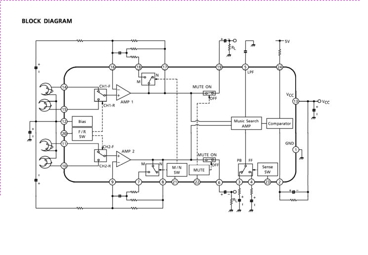
The TA2042F is a dual preamplifier with a music interval detection circuit designed for auto-reverse car stereo systems. This integrated circuit (IC) features dual amplifiers, a forward/reverse control switch, and a metal/normal tape equalizer. The TA2042F serves as a pivotal...
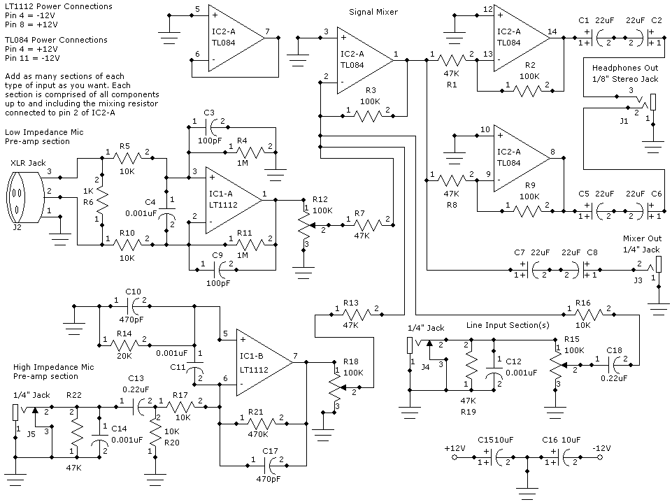
This weblog focuses on electronic circuit schematics, PCB design, DIY kits, and diagrams for various electronic projects. It features a mixer that demonstrates how to create microphone pre-amplifiers suitable for both low and high impedance microphones. The design utilizes...
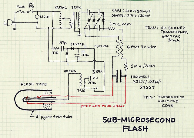
The two resistors serve dual purposes. Firstly, they limit the current to a lower value in case of accidental contact with the circuit. Secondly, when the flash is activated, the main capacitor behaves like a short circuit to the...
The amplifier circuit utilizing the STK4050 integrated circuit (IC) is known for its robustness and high quality. This article presents a 200-watt power amplifier circuit based on the STK4050. The circuit features an advanced auto wiring diagram with color-coded...