
PNP Transistor Analysis

The PNP transistor is a type of bipolar junction transistor (BJT) characterized by its construction and operational principles, which are fundamentally the reverse of those found in NPN transistors. In a PNP transistor, the emitter (E) is connected to a positive voltage supply (VCC), while the collector (C) is connected to the load and the base (B) is biased negatively. This configuration allows the PNP transistor to conduct when the base is at a lower potential than the emitter, typically requiring a base-emitter voltage (VBE) of around -0.7V for silicon devices or -0.3V for germanium devices.
In terms of circuit design, the PNP transistor operates effectively in various configurations, including common emitter, common base, and common collector. In the common emitter configuration, the PNP transistor acts as a current amplifier, where a small base current controls a larger collector current. The load resistor (RL) in the collector circuit limits the maximum current, ensuring the transistor operates within safe limits.
The output characteristics of a PNP transistor can be analyzed using its I-V curves, which are analogous to those of an NPN transistor but inverted due to the opposite polarity of voltages and current directions. The load line analysis on these curves helps in determining the operating points of the transistor under different conditions, allowing for effective design and optimization in amplifier circuits.
In summary, the PNP transistor's unique characteristics and operational principles make it a crucial component in electronic circuit design, particularly in applications requiring complementary transistor configurations, such as push-pull amplifiers, where both NPN and PNP transistors work together to achieve efficient amplification.The PNP Transistor is the exact opposite to the NPN Transistor device we looked at in the previous tutorial. Basically, in this type of transistor construction the two diodes are reversed with respect to the NPN type giving a Positive-Negative-Positive type configuration, with the arrow which also defines the Emitter terminal this time pointing in
wards in the transistor symbol. Also, all the polarities for a PNP transistor are reversed which means that it sinks current into its Base as opposed to the NPN transistor which sources current through its Base. The main difference between the two types of transistors is that holes are the more important carriers for PNP transistors, whereas electrons are the important carriers for NPN transistors.
Then, PNP transistors use a small base current and a negative base voltage to control a much larger emitter-collector current. In other words for a PNP transistor, the Emitter is more positive with respect to the Base and also with respect to the Collector.
The construction and terminal voltages for an NPN transistor are shown above. The PNP Transistor has very similar characteristics to their NPN bipolar cousins, except that the polarities (or biasing) of the current and voltage directions are reversed for any one of the possible three configurations looked at in the first tutorial, Common Base, Common Emitter and Common Collector. The voltage between the Base and Emitter ( VBE ), is now negative at the Base and positive at the Emitter because for a PNP transistor, the Base terminal is always biased negative with respect to the Emitter.
Also the Emitter supply voltage is positive with respect to the Collector ( VCE ). So for a PNP transistor to conduct the Emitter is always more positive with respect to both the Base and the Collector. The voltage sources are connected to a PNP transistor are as shown. This time the Emitter is connected to the supply voltage VCC with the load resistor, RL which limits the maximum current flowing through the device connected to the Collector terminal.
The Base voltage VB which is biased negative with respect to the Emitter and is connected to the Base resistor RB, which again is used to limit the maximum Base current. To cause the Base current to flow in a PNP transistor the Base needs to be more negative than the Emitter (current must leave the base) by approx 0.
7 volts for a silicon device or 0. 3 volts for a germanium device with the formulas used to calculate the Base resistor, Base current or Collector current are the same as those used for an equivalent NPN transistor and is given as. We can see that the fundamental differences between a NPN Transistor and a PNP Transistor is the proper biasing of the transistors junctions as the current directions and voltage polarities are always opposite to each other.
So for the circuit above: Ic = Ie Ib as current must leave the Base. Generally, the PNP transistor can replace NPN transistors in most electronic circuits, the only difference is the polarities of the voltages, and the directions of the current flow. PNP transistors can also be used as switching devices and an example of a PNP transistor switch is shown below.
The Output Characteristics Curves for a PNP transistor look very similar to those for an equivalent NPN transistor except that they are rotated by 180o to take account of the reverse polarity voltages and currents, (the currents flowing out of the Base and Collector in a PNP transistor are negative). The same dynamic load line can be drawn onto the I-V curves to find the PNP transistors operating points.
You may think what is the point of having a PNP Transistor, when there are plenty of NPN Transistors available that can be used as an amplifier or solid-state switch. Well, having two different types of transistors PNP and NPN , can be a great advantage when designing power amplifier circuits such as the Class B Amplifier.
🔗 External reference
Related Circuits
A straightforward method to create a speaker transformer involves winding turns around a ferrite rod. The primary winding consists of 300 turns of 0.01mm wire, which is very fine, wound over the secondary and concluding with a loop of...
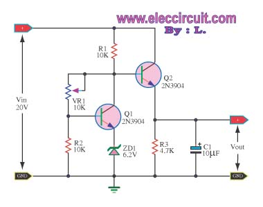
This circuit maintains a constant voltage, with an adjustable output voltage. It serves to reduce the input voltage while keeping the voltage constant. The amplifier model used is the Q1 2N3904 in a common-emitter configuration. This configuration allows the...
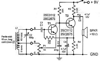
This circuit is a simple one-transistor Audion type radio powered by a 1.5 V battery. It utilizes a pair of standard low-impedance headphones, wired in series to achieve a total impedance of 64 ohms. The power supply to the...
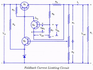
If the load resistance (RL) is reduced or the load terminals are accidentally shorted, a very large load current will flow, potentially damaging the pass transistor (Q1), diode, or other components. Fuse protection may not be sufficient, as the...
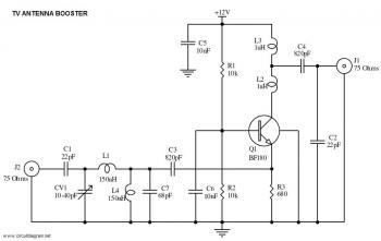
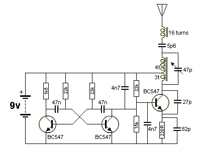
This is a straightforward circuit for a UHF band TV antenna booster that provides a gain of 15 dB. This low-cost antenna booster is simple and easy to construct. The UHF band TV antenna booster circuit is designed to enhance...
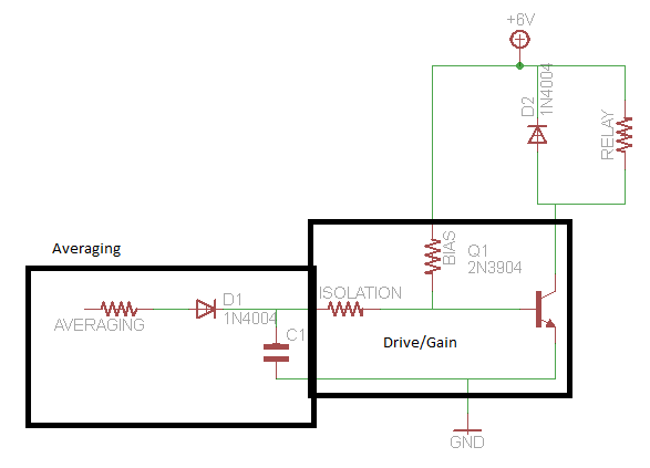
A circuit that activates a relay upon detecting audio pulses from one channel of an MP3 player. The intention is to synchronize recorded audio pulses with music to control a motor for mouth movement. For a stereo player, music...