
DC Voltage Regulator Circuit

The circuit design employs a pulse width modulation (PWM) technique to regulate the output voltage. The A1 operational amplifier is configured in a way that it generates a square wave signal, which is essential for the PWM operation. The triangle wave signal, which is typically generated by a function generator or another op-amp configured in a triangular mode, is fed into the non-inverting input of the A1 op-amp. The output of A1 oscillates between high and low states, effectively creating the PWM signal.
The A2 comparator takes the square wave output from A1 and compares it with a reference voltage set by the potentiometer P1. The adjustment of P1 allows for fine-tuning of the duty cycle of the PWM signal, which directly influences the average voltage delivered to the load. This adjustable reference voltage is critical for applications requiring precise control over the output power.
Transistor T1 is utilized as a switching element in this circuit. When the PWM signal from A2 turns on T1, it allows current to flow to the load, which could be any device such as a motor or LED. The ability of T1 to handle up to 5 amperes makes this circuit suitable for moderate power applications. The choice of transistor must also consider the switching speed and thermal characteristics to ensure reliable operation under varying load conditions.
The power supply requirements for this circuit are flexible, with a range of 5 to 30 volts. However, it is crucial to understand that efficiency decreases as the supply voltage approaches the lower limit. This is due to the inherent losses in the regulation process and the characteristics of the components used. Therefore, for optimal performance, it is advisable to operate the circuit within the mid-range of the specified voltage limits.
In summary, this DC power regulation circuit is versatile and effective for various applications that require precise control of voltage and current through PWM. Its design incorporates standard components, making it accessible for implementation in both experimental and practical scenarios.This circuit regulates a DC power output. It has a very wide application range. It can be used to control the speed of a motor, a pump, a toy train, the brightness of a LED or lamp, etc. Practically, it can be used in any application that uses a regulated DC power with pulse width modulation (PWM).
The circuit works this way: the A1 opamp function s as a square wave generator. At its non-inverting input is a by product triangle wave signal. The IC A2 following it functions as a simple comparator. A reference voltage is fed to the inverting input of the A2 IC via the potentiometer P1. The output of A2 is a square wave signal with a constant frequency of around 200 Hertz. The P1 sets the trigger point of the pulse. The transistor T1 works as the actual regulator by switching a relatively high current with a maximum of 5 amperes. The power supply voltage must be between 5 volts (minimum) and 30 volts (maximum). Take note that the lower the supply voltage is, the lower the efficiency of the dc regulator becomes.
🔗 External reference
Related Circuits
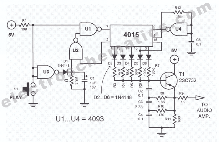
This circuit is a musical doorbell. When the button S1 is pressed, a short melody plays. If the button is pressed multiple times in quick succession or held down, a different melody is generated, and the melody plays for...
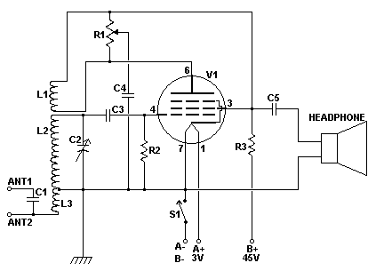
A regenerative radio operates by feeding back a small portion of the amplified output from the detector into the input. This feedback mechanism enhances sensitivity significantly beyond what a detector can achieve on its own. The simple regenerative radio...
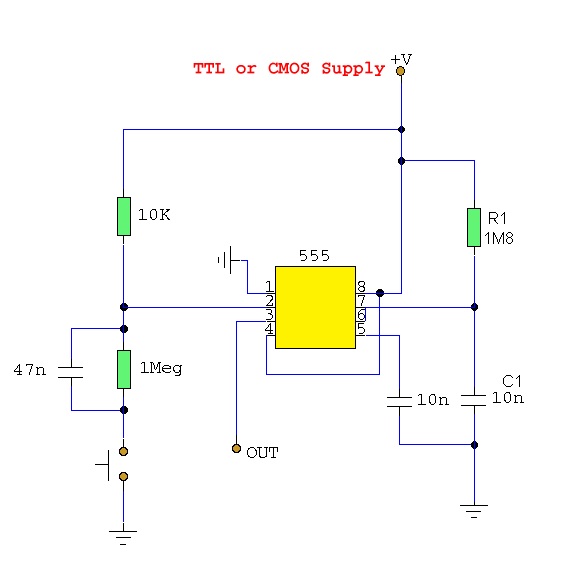
The 555 circuit can be re-triggered if the input is held low for a duration longer than the output pulse. To prevent this from occurring, an additional timing circuit has been incorporated, consisting of a 1 Megohm resistor and...

The diagram below illustrates a Two Phase Bipolar Stepper Motor Driver utilizing the PBL3717A. It depicts two PBL3717A integrated circuits (ICs) that control and drive two bipolar stepper motors. The Two Phase Bipolar Stepper Motor Driver circuit is designed to...
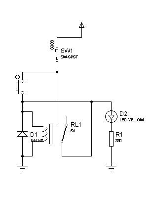
The circuit can also be triggered by logic ICs (TTL/CMOS) using the appropriate interfacing method. Another relay is typically used to serve as the trigger button when interfacing ICs with the latching relay circuit. The described circuit utilizes a latching...
MOSFETs cannot simply be connected to the drive signal and expected to function correctly. Due to their construction, driving MOSFETs can be complex, particularly for beginners. Many users frequently seek assistance with MOSFET drive issues on various blogs, websites,...