
Power down function

This circuit design employs a power management strategy to enhance the reliability and performance of analog I/O ports, specifically targeting devices such as the AD7769 and AD7774. The primary function of this circuit is to provide a controlled power-down capability while eliminating the need for protective diodes typically used to guard against power-supply missequencing.
The operation of the circuit hinges on a power-down control signal that, when asserted high at +5V, activates the power supply to the connected analog components by turning on the associated MOSFETs. The control mechanism involves two cross-coupled NOR gates (U1C and U1D), which orchestrate the switching of the +5V and +12V supplies through MOSFETs Q1 and Q2, respectively. This strategic sequencing is crucial, as improper power application can lead to damage of sensitive components.
Upon activating the power-down control, the output of U1C transitions to a low state, which initiates the discharge of capacitor C1 through resistor R1. The discharge follows an exponential decay characterized by the time constant R1C1. As the voltage across C1 decreases, it triggers additional events within the circuit, although these specific events are not detailed in the provided description.
The design effectively ensures that the power-up and power-down sequences are carefully managed to prevent any adverse effects on the controlled circuits, thereby enhancing the overall robustness of the system. This approach is particularly beneficial in applications where power sequencing is critical for the operational integrity of the devices involved. This circuit adds a power down function to analog I/O ports (for example, the AD7769 and AD7774). Moreover, the diodes ordinarily needed to protect the devices against power-supply missequencing can be eliminated Bringing the power down control high (+5V) applies power to the controlled circuit by turning on all MOSFETs. Specifically, raising the power down brings the output of U1C low, causing capacitor C1 to discharge VOL exponentially with time constant R1C1.
As the voltage on C1 falls, two events occur. In the circuit, MOSFETs Q1 and Q2 switch the +5- and +12-V supplies, respectively, in a sequence controlled by two cross-coupled CD4001 CMOS NOR gates (U1C and U1D). The sequence in which power isapplied is important: The controlled circuits may be dama 🔗 External reference
Related Circuits
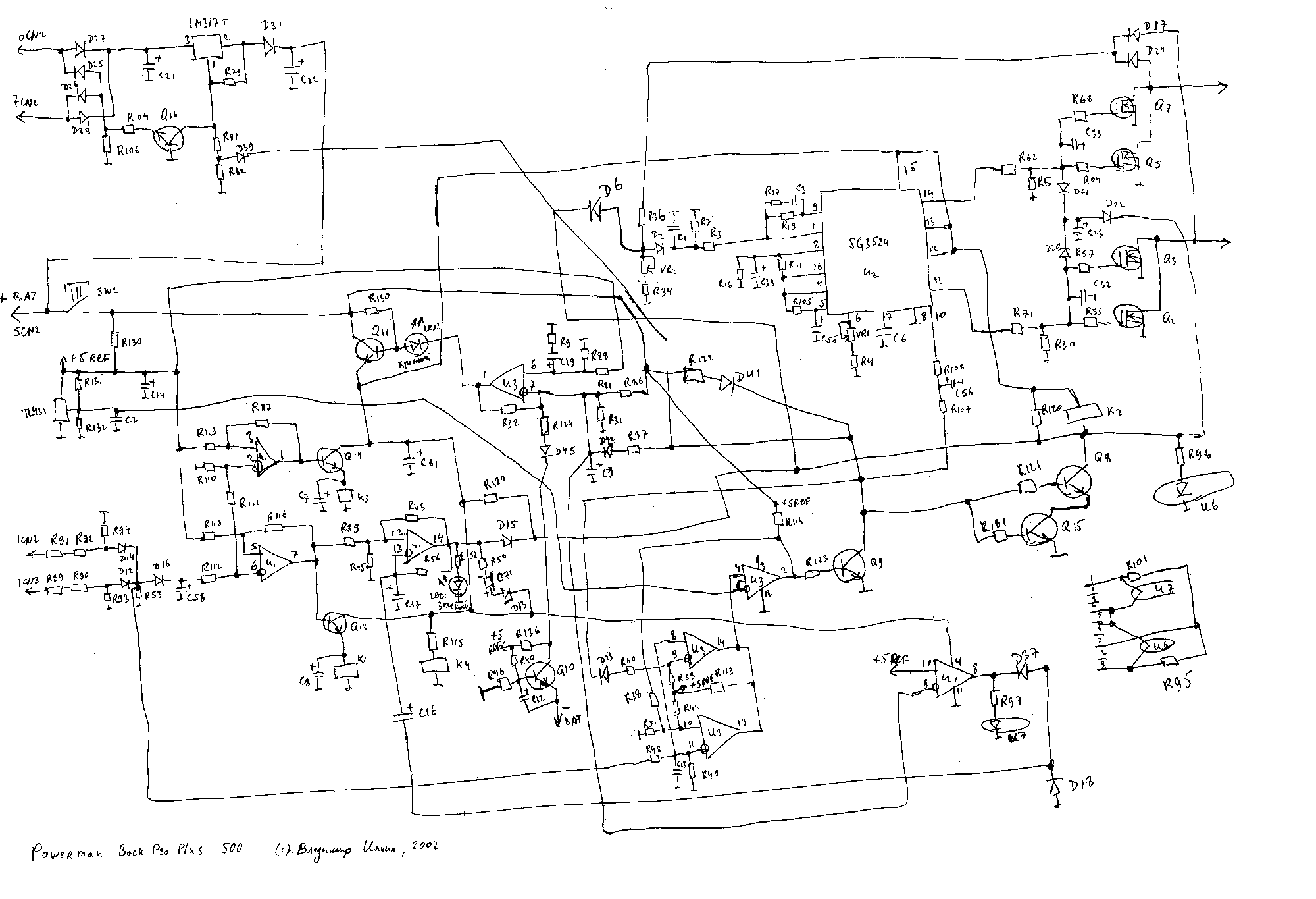
PowerMan UPS/Inverters manufactures uninterruptible power supplies and voltage regulators. The business was founded in 1993 and was involved in distribution prior to the year 2000. PowerMan specializes in providing reliable power solutions, including uninterruptible power supplies (UPS) and voltage regulators,...
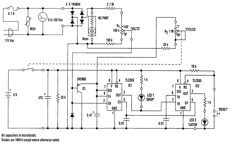
The 0 to 130-volt voltmeter and neon "AC PWR" lamp provide an average indication of AC power. The fuse and metal oxide varistor (MOV) protect the monitor against overvoltage spikes. Four 1N4004 diodes rectify the AC voltage, generating negative-going...
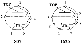
Vacuum Tubes 807 and 1625 are commonly used by hams as power amplifiers. Both tubes are audio power amplifier beam tetrodes in the output stage of high power amplifiers but they are suitable for high frequencies also. Both tubes...
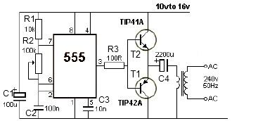
This 12V power inverter circuit can be utilized to power small devices that require 240 volts. It is particularly advantageous for operating 240-volt appliances using a 12-volt car battery. Unlike typical feedback oscillator inverters, this design employs a 555...

An electronic rectification circuit that avoids the use of large, heavy, and expensive electrolytic capacitors by utilizing an active transistor in a gyrator configuration. To minimize excess ripple output on a power supply feeding a heavy load, a large...
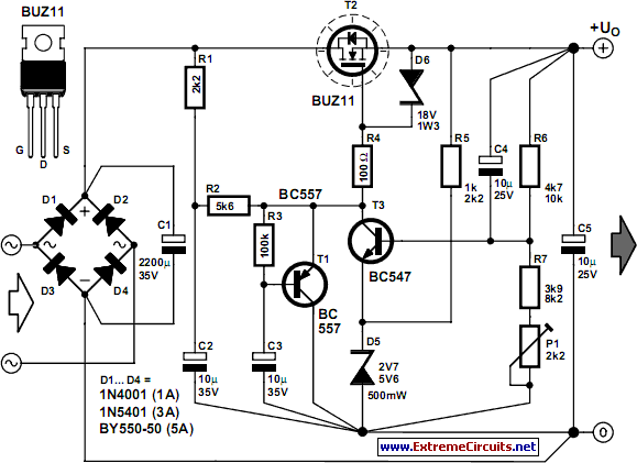
The circuit diagram illustrates a voltage regulator designed from discrete components to meet specific voltage requirements. It provides two sets of component values for output voltages of 6.3 V (upper) and 12.6 V (lower). The components used include BC547...
Warning: include(partials/cookie-banner.php): Failed to open stream: Permission denied in /var/www/html/nextgr/view-circuit.php on line 713
Warning: include(): Failed opening 'partials/cookie-banner.php' for inclusion (include_path='.:/usr/share/php') in /var/www/html/nextgr/view-circuit.php on line 713