
Practical three control delay self-extinguishing switch circuit schematics
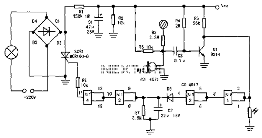
1. Power Circuit: This section consists of diodes D1, D2, D3, D4, resistors R1, R2, and capacitor C1. The diodes form a bridge rectifier circuit that converts 220V AC from the load (light bulb) into DC. The DC voltage is then stepped down and filtered by resistors R1, R2, and capacitor C1, which provides a supply voltage of approximately 9.5V to the subsequent unit circuit.
2. Signal Conversion Detecting Circuit: This circuit detects light, sound, and touch signals. Light detection is achieved using a photoresistor (RC) and resistor R5, which alters the voltage across the resistor based on light intensity. This voltage is sent to the integrated circuit CD4071 at pins 1 and 2 for processing. Sound detection is facilitated by an electret microphone (MIC), along with capacitors C3 and resistors R4, R5, and R6. The microphone converts sound signals into electrical signals, which are amplified by transistor Q1. The presence or absence of sound modifies the voltage at the collector of Q1, which is then processed by the CD4071. Touch detection is accomplished through a touch sheet, with signals entering Q1 for amplification and subsequently reaching pins 1 and 2 of the CD4071. The interaction of sound and touch signals results in voltage changes at these pins.
3. Delay Circuit: This circuit consists of diode D5, resistor R7, and capacitor C2. Resistor R7 and capacitor C2 control the delay time, which is approximately 150 seconds as indicated in the schematic. Diode D5 prevents capacitor C2 from discharging to pin 4 of the CD4071 during the delay period.
4. Control Circuit: The control circuit is formed by the integrated circuit CD4071, a single thyristor (SCR1), and resistor R8. The CD4071 functions as a four-input OR gate, allowing for the integration of the various signals processed from the previous circuits.
This comprehensive description outlines the functionality and components of the sound, light, and touch-controlled delay self-extinguishing switch circuit. Each segment plays a critical role in ensuring the circuit operates effectively, providing both control and safety features. Circuit The figure is sound, light, touch control delay self-extinguishing switch three electrical schematic diagram of the circuit from the power circuit, the signal conversio n detecting circuit, a delay circuit and a control circuit. 1. circuit (1) power circuit. The circuit consists of a diode Dl, D2, D3, D4, resistors Rl, R2 and capacitor Cl form. Wherein D1 ~ D4 form a bridge rectifier circuit, its function is through the load (light bulb) of 220V AC to DC, the DC high voltage, Rl, R2 and Cl complete the pulsating DC voltage rectified step-down and filtering. Cl is the voltage at both ends of the subsequent unit circuit supply voltage of approximately 9.5V. (2) converting the signal detection circuit. The circuit includes light, sound and touch the human body detection signal conversion. Wherein the light is detected by the photoresistor RC R5 and composition, the photosensitive voltage across the resistor changes with the intensity of the light changes, and sent to the integrated circuit CD4071 1,2 feet for processing; the sound is detected by the electret microphone MIC, C3, R4, R5, R6 and Ql composition, the sound signal is converted to electrical signals by the MIC capacitor C3 is coupled to the amplifying transistor Ql, resistors R4, R5 constitute Ql DC bias resistance, presence or absence of sound through the collector of Ql voltage change to the first integrated circuit CD4071 1,2 feet treated for biasing resistor R6 amplifying elements inside the MIC; human touch sensing signal through the touch sheet, R3, C3 enter Ql amplification, and from the C Ql pole input to the CD4071 1,2 feet, when the presence or absence of a touch signal will cause CD4071 1,2 feet voltage changes, voltage thus CD4071 1,2 feet is the result of a signal by the sound and the touch interaction.
(3) delay circuit. The circuit consists of D5, R7 and C2. Wherein R7 and C2 for the delay time control element, the delay time parameters shown in FIG approximately 150s. Diode D5 function is to prevent C2 to CD4071 4 feet Discharges delay time. (4) control circuit. The circuit consists of integrated circuit CD4071, one-way thyristor SCR1 and R8 components. Wherein CD4071 is four hundred and twelve input OR gate.
Related Circuits
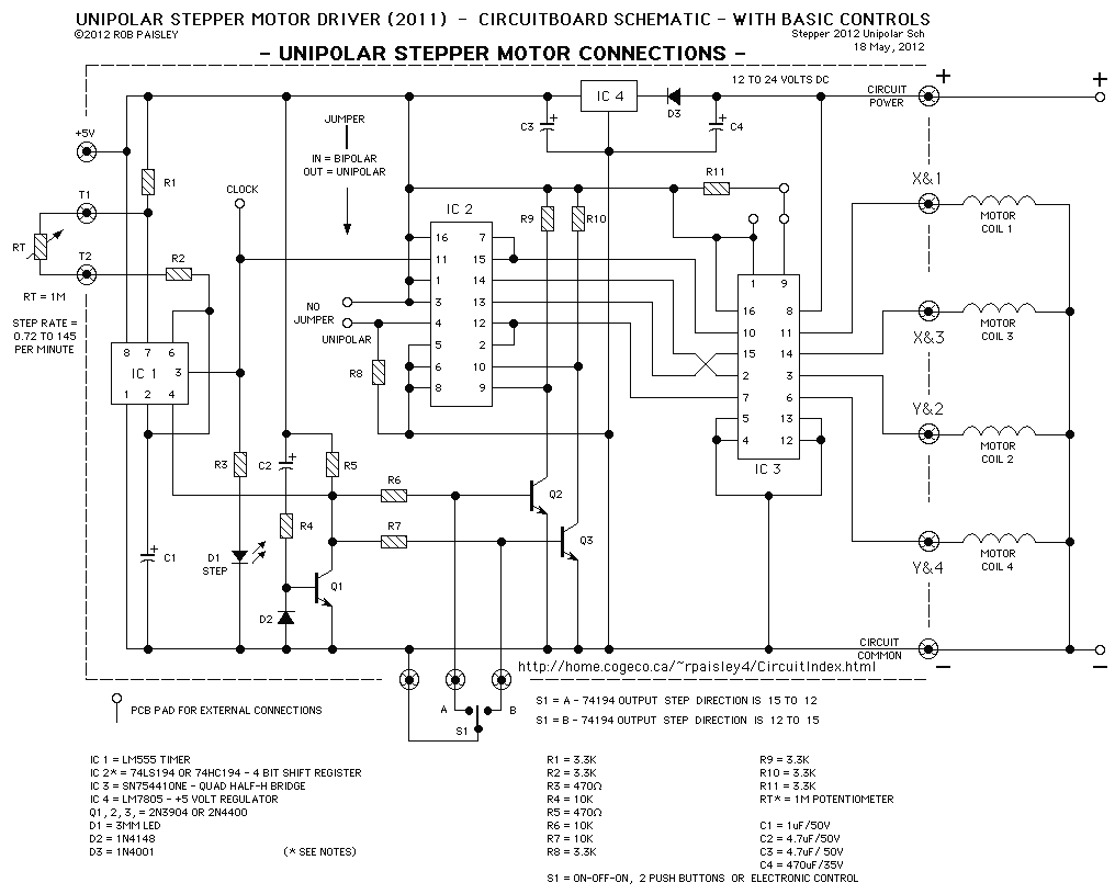
The following diagram is for the main circuit of the motor driver. A testing version is shown near the end of this page. It is laid out differently and shows the SN7474 in logic block form and LEDs are...
Carefully examine the following circuit diagram and attempt to construct the circuit on a breadboard first. If it functions correctly, proceed to create its PCB version. The circuit diagram serves as a blueprint for constructing an electronic circuit on a...
The schematic for controlling the motors is divided into three main sections, each serving a distinct function. The primary components featured in the schematic include the PIC 18F252 microcontroller, the SN754410 motor driver, and 2N2222 transistors. At the top...
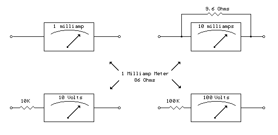
A milliamp meter can function as a voltmeter by incorporating a series resistance. The required resistance is calculated by dividing the full-scale voltage reading by the full-scale current of the meter movement. For instance, using a 1 milliamp meter...
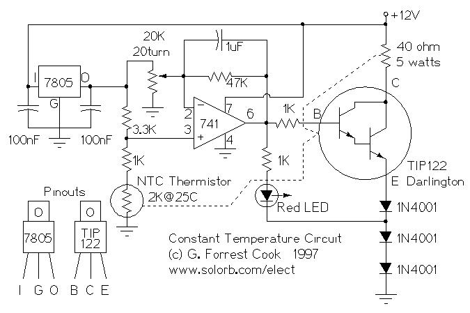
Constant Temperature Circuit. G. Forrest Cook 1997. Introduction: This circuit is a generic low-power temperature controller that can be used for stabilizing temperature. The constant temperature circuit described is designed to maintain a stable temperature in various applications, utilizing low...
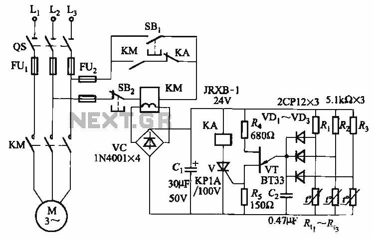
The thyristor control circuit includes a bridge circuit designed to regulate the temperature in the contactor coil KM, along with a secondary winding that functions as a power protection device. It comprises a thermistor (R:., Rt3) and a resistor...