
Precision buffered reference
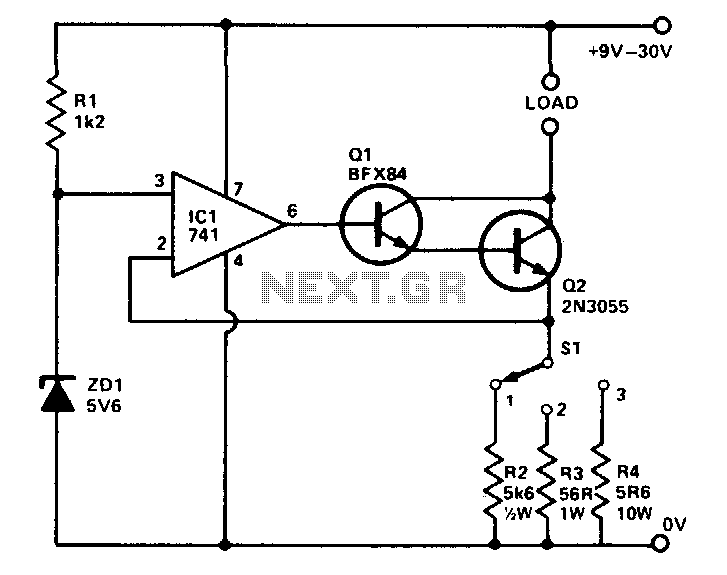
The circuit described operates as a constant current source, which is crucial for applications requiring stable current levels regardless of fluctuations in temperature or supply voltage. The primary component, ZD1, functions as a Zener diode that provides a stable reference voltage, which is essential for maintaining the integrity of the circuit's operation. This reference voltage is fed into the non-inverting input of operational amplifier IC1, which compares it with the feedback voltage from the output.
The feedback mechanism employed in this circuit is vital for its functionality. By applying 100% feedback from the output to the inverting input of IC1, the circuit effectively creates a control loop that adjusts the output voltage to match the reference voltage. This ensures that the voltage at the emitter of transistor Q2 remains consistent with the reference voltage, thereby stabilizing the output current.
The selection of current levels is facilitated by the resistor connected to switch S1. By changing the resistor value, the user can select between the preset currents of 10 mA, 100 mA, or 1 A. This versatility makes the circuit adaptable for various applications, from powering small sensors to driving larger loads.
Thermal management is also a critical consideration in this design. Transistor Q2, which handles the load current, should be mounted on an appropriate heatsink to dissipate excess heat generated during operation. This thermal management ensures that the transistor operates within safe limits, preventing thermal runaway and maintaining the reliability of the circuit over prolonged use.
Overall, this circuit design exemplifies a robust solution for applications requiring stable and adjustable current sources, with built-in safeguards against environmental fluctuations and thermal issues.The circuit will provide 3 preset currents which will remain constant despite variations of ambient temperature or line voltage. ZDl produces-a temperature stable reference voltage which is applied to the noninverting input of ICl.
100% feedback is applied from the output to the inverting input holding the voltage at Q2s emitter at the same potential as the noninverting input. The current flowing into the load therefore is defined solely by the resistor selected by Si With the values employed here, a preset current of 10 mA, 100 mA or 1 A can be selected. Q2 should be mounted on a suitable heats ink. 🔗 External reference
Related Circuits
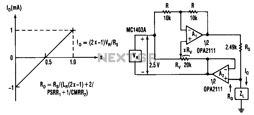
This current source provides continuous control over the magnitude and polarity of its amplifier gain, requiring only a single voltage reference. The circuit comprises a voltage-amplifier circuit (A1) with a gain-setting resistor (Rs) and a bootstrap-follower amplifier (A2). The...
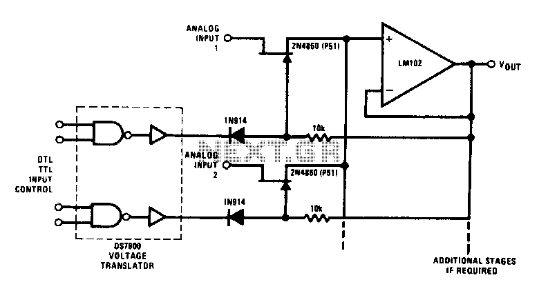
This analog switch utilizes the 2N4860 JFET, which features a low on-resistance of 25 ohms and minimal leakage current. The LM102 is employed as a voltage buffer in the circuit. Additionally, this configuration can be modified for use in...
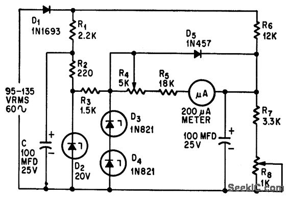
This circuit measures alternating current (AC) voltages in the range of 95 to 135 volts with an accuracy of 0.6%, utilizing a standard meter that has a 2% accuracy rating. The circuit employs Zener diodes to provide a stable...
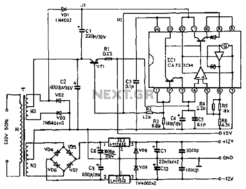
The circuit depicted features a secondary N3 center tap transformer (T) with a common point connecting diodes VD2 and VD3 to positive electrodes, along with capacitors C2, C6, C7, and negative electrodes connected to capacitors C9 and C10. Additional...
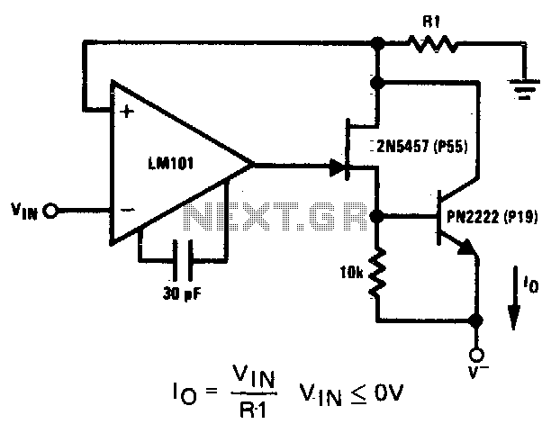
The 2N5457 and PN2222 bipolar transistors function as voltage isolation devices between the output and the current sensing resistor, Rl. The LM101 operational amplifier offers a significant amount of loop gain to ensure that the circuit operates as a...
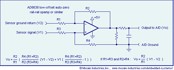
Ground loop offset errors and ground noise are eliminated by a differential amplifier or instrumentation amplifier before the analog-to-digital (A/D) conversion. The differential input amplifier addresses ground loop errors, allowing for precise measurement of non-isolated sensors. A simple operational...
Warning: include(partials/cookie-banner.php): Failed to open stream: Permission denied in /var/www/html/nextgr/view-circuit.php on line 713
Warning: include(): Failed opening 'partials/cookie-banner.php' for inclusion (include_path='.:/usr/share/php') in /var/www/html/nextgr/view-circuit.php on line 713