
Precision Amplifiers
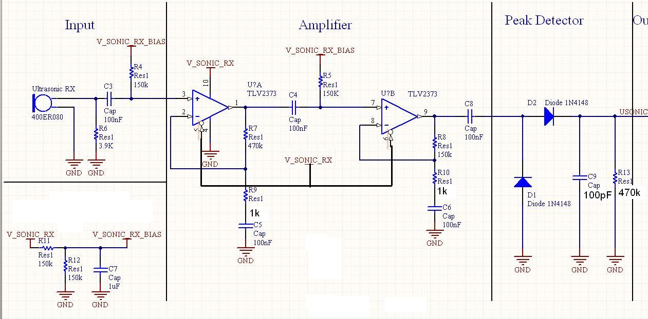
To analyze the situation, it is essential to understand the configuration and functionality of the operational amplifiers involved. The op amp in question, when tested in a buffer configuration, should ideally provide a straightforward output that reflects the input voltage, confirming whether the device is operational. If the output deviates significantly from the expected behavior, it may indicate a fault within the op amp itself.
The voltage discrepancies noted at V_SONIC_RX_BIAS2, pin 7, and V_SONIC_RX suggest that there may be issues with the biasing or potential dividers within the circuit. The difference in voltage levels between op amp A and op amp B could be indicative of varying load conditions or feedback configurations affecting their performance. The non-inverting configuration of the op amps should produce specific gain characteristics, and any deviation in output suggests that further investigation into the circuit layout, component values, and connections is warranted.
Furthermore, it is advisable to perform a thorough examination of the surrounding circuitry, including any resistors, capacitors, or other components that may influence the operation of the op amps. By isolating each stage of the circuit and confirming the integrity of each component, a clearer understanding of the root cause of the discrepancies can be achieved, leading to a more effective troubleshooting process.Also you have mentioned that the op amp in the second stage gets damaged. Can you confirm that by testing that op amp in a buffer configuration(or any simple configuration) I am asking you to do this because we need to know if the part is actually failing or is it something else in the circuitry which is causing it to behave like this. I see. But why the potential at V_SONIC_RX_BIAS2 is 1. 8V and at pin 7 is 2. 5V while the V_SONIC_RX is 3. 0V and why is this different from the op amp-A (1. 5V on bias voltage and pin 3 of op amp-A). u also see the photos in my previous emails when the op amp is in non-inverting configuration. op amp A vs op amp B. the output of op amp B is different from output of op amp A. 🔗 External reference
Related Circuits
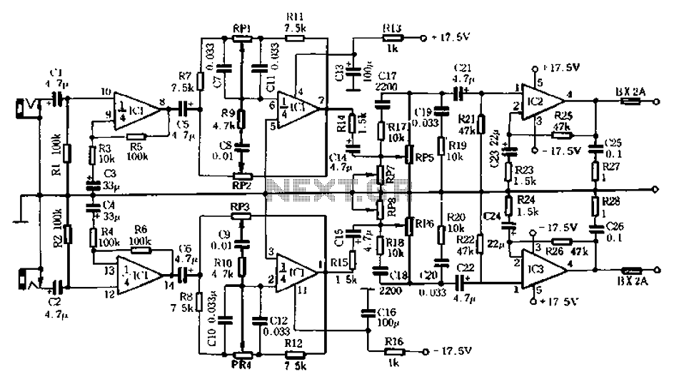
The circuit depicted in Figure 5-60 and Figure 6 utilizes an operational amplifier (op-amp) configured as a channel pre-amplifier to address the signal loss introduced by the tone control circuit. Additionally, another group of op-amps forms a channel-driven stage...
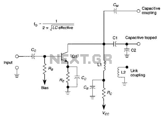
This basic tuned LC amplifier can be used with three output coupling methods: capacitive coupling output, capacitive tapped output, or link-coupled output. The tuned LC amplifier is a fundamental circuit used in various applications, including radio frequency (RF) amplification and...
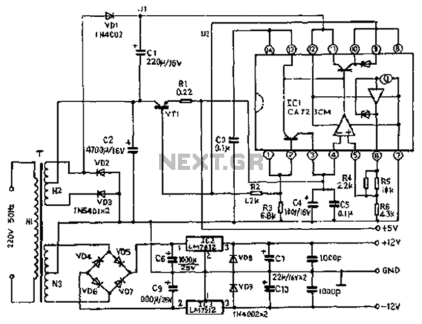
The circuit depicted features a secondary N3 center tap transformer (T) with a common point connecting diodes VD2 and VD3 to positive electrodes, along with capacitors C2, C6, C7, and negative electrodes connected to capacitors C9 and C10. Additional...
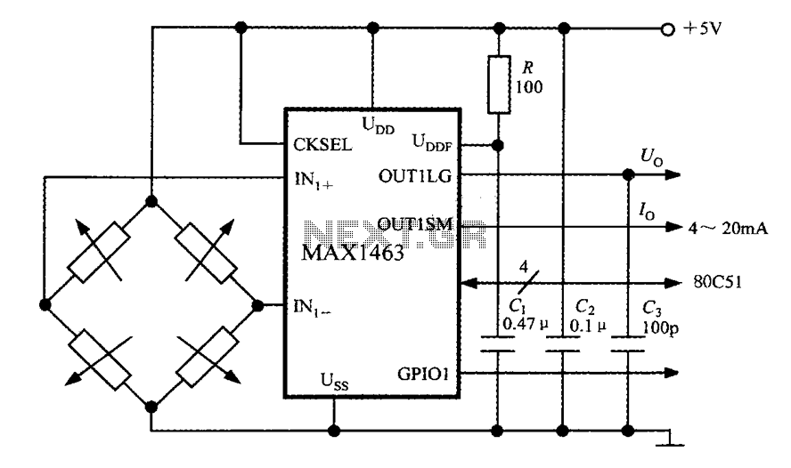
The system consists of a MAX1463 precision pressure detection circuit block diagram. The output voltage from the bridge pressure sensor is connected to the MAX1463 inputs IN1+ and IN1-. Controlled by a CPU, the pressure signal undergoes nonlinear calibration...
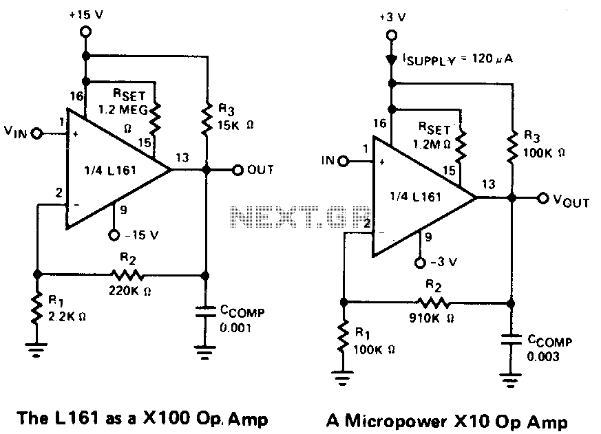
This is a single gain-of-100 amplifier with a gain-bandwidth product of 20 MHz. The primary limitation in performance is the low slew rate of 0.3 V/μs imposed by the charging of Ccomp. The effects of slew rate and compensation...
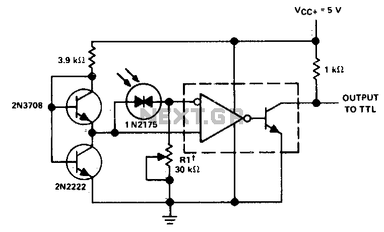
Rl sets the comparison level. At comparison, the photodiode has less than 5 mV across it, decreasing dark current by an order of magnitude. More: IC = LM 111/211/311. In this circuit description, the resistor Rl plays a crucial role...