
Precision Full-Wave Rectifier
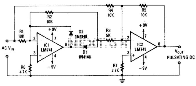
The described circuit employs two operational amplifiers to achieve full-wave rectification, a process that allows both halves of an AC waveform to contribute to the output. The first operational amplifier, designated as IC1, functions as an inverter. When the input signal is negative, IC1 inverts this signal; however, diode D2 ensures that the output remains at a near-zero level, preventing the output from dropping too low.
The second operational amplifier, IC2, takes the output from IC1 and the positive signal derived from the resistive network formed by R4 and R5. The configuration ensures that during the positive half-cycle of the input signal, IC1 produces a negative output through diode D1, which is then fed into IC2.
At the summing junction of IC2, the circuit combines the inverted output from IC1 with the positive signal from the resistors. The resistors R3 and R5 play a crucial role in determining the gain and the summation effect at the output. The negative output from IC1 is effectively doubled and inverted in IC2, leading to a resultant positive output voltage, denoted as +Vout. This output is then summed with the negative output of IC1 to produce the final output, which is also +Vout.
This arrangement results in a full-wave rectified output, effectively allowing the circuit to convert an AC input signal into a DC equivalent, with both positive and negative halves of the waveform contributing to the output. The design is particularly useful in applications where a smooth DC voltage is required from an AC source, such as in power supply circuits or signal processing applications. Using two op amps, this circuit produces a full-wave rectified version of the input signal. Op amp IC1 invert s the negative-going signal, but because of D2, it stays near zero. IC2 produces a positive-going signal. For positive-going signals, IC1 produces a negative output through Dl to IC2, where it is combined with positive from R4/R5. At the summing junction of IC2, the negative output of IC1 is doubled and inverted via IC2, R3, and R5 to produce + V0ut- This is summed with negative output of IC1 to produce +Vout.
🔗 External reference
Related Circuits
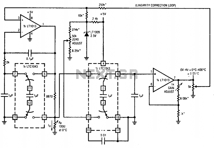
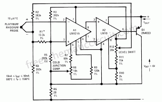
The circuit provides complete, linearized signal conditioning for a platinum RTD. This LTC1043-based circuit is considerably simpler than instrumentation or multi-amplifier based designs and operates from a single 5 V supply. Amplifier A1 serves as a voltage-controlled, ground-referred current...
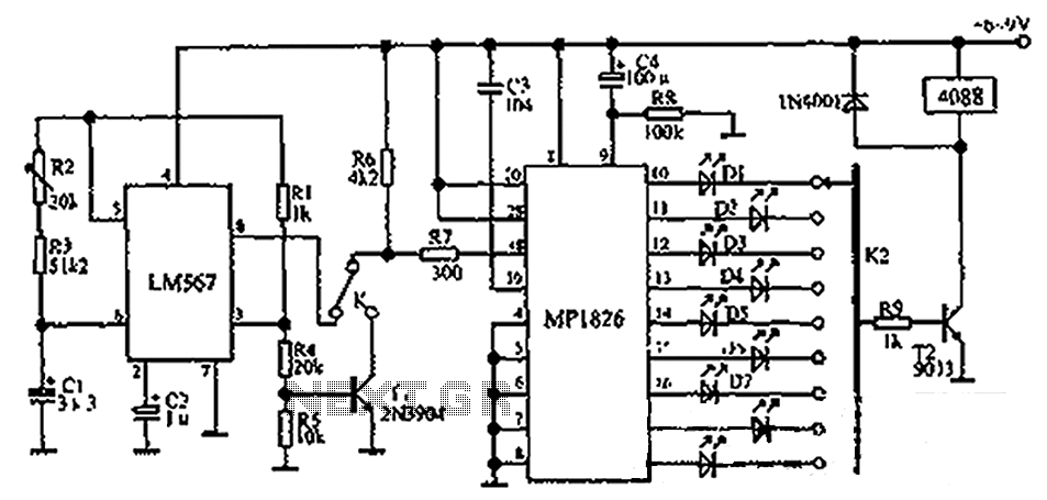
The circuit illustrated in the figure incorporates the MP1826 as a multi-stage divider. The LM567 serves as the frequency demodulation component, functioning as a dual-band oscillator that generates the desired low-frequency pulse from the MP1826. The oscillation center frequency...
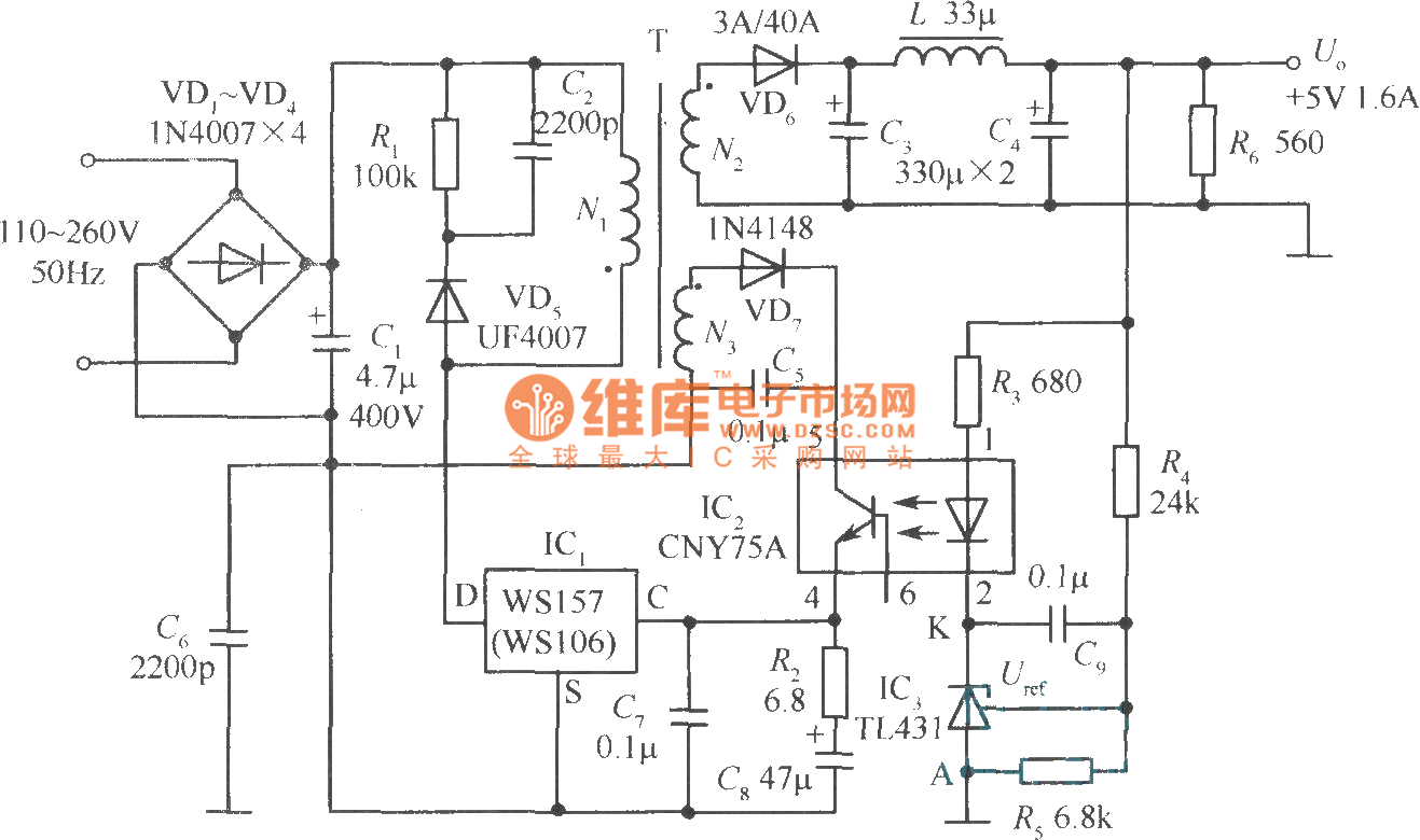
The +5V, 1.6A precision switching power supply circuit is depicted in the figure. This circuit utilizes a photoelectric coupler (CNY75A) and an adjustable precision parallel regulator (TIA31). R3 serves as the current limiting resistor, while R4 and R5 function...
This circuit demonstrates how a low-drift preamplifier can enhance the measurement resolution of a thermocouple. The preamplifier is powered by the reference regulator, and bridge feedback is employed to bias the preamplifier input within its common mode range. Cold...
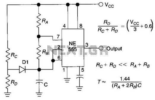
Using Rl, R7, and D1 to preset CI to one third of the supply voltage. This circuit avoids a longer first cycle period than subsequent cycles. The circuit described involves the use of resistors Rl and R7 along with diode...
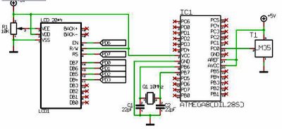
The LM35 series used in this project is a precision centigrade temperature sensor with an analog output voltage. It has a temperature range of -55 °C to +150 °C and an accuracy of ±0.5 °C. The output voltage is...