
Programmable Inverter/Rectifier
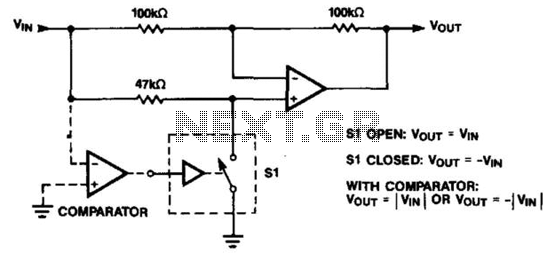
The described circuit utilizes an operational amplifier (op amp) configured to operate in two distinct modes: inverter and buffer. The mode of operation is controlled by a switch that alters the polarity of the input signal. In buffer mode, the op amp provides a high input impedance and a low output impedance, ensuring that the input signal is accurately reproduced at the output without any amplification or attenuation, maintaining a unity gain of 1.
When configured as an inverter, the op amp inverts the input signal, and the gain is determined by the feedback network composed of resistors. The relationship between the input voltage (Vin) and the output voltage (Vout) can be expressed as Vout = - (Rf/Rin) * Vin, where Rf is the feedback resistor and Rin is the input resistor. This configuration allows for various gain settings based on the selected resistor values, enabling the circuit to adapt to different signal conditioning requirements.
Incorporating a comparator into the circuit enhances functionality, allowing for synchronous switching of the op amp's mode based on the input signal's polarity. The comparator compares the input signal with a reference voltage, and when a threshold is crossed, it triggers the switch to change the op amp's configuration. This mechanism effectively rectifies the output, producing a unidirectional signal that can be useful in applications such as signal processing and waveform shaping.
The output polarity of the circuit is determined by the logic state of the switch, which can be configured as normally open (NO) or normally closed (NC). In a normally open configuration, the circuit operates in buffer mode until the switch is activated, at which point it transitions to inverter mode. Conversely, in a normally closed configuration, the inverter mode is active until the switch is deactivated. This flexibility allows for dynamic control of signal processing based on real-time input conditions, making the circuit suitable for various electronic applications. The op amp is alternately an inverter or buffer, under control of the switch polarity. As a buffer, the gai n is always 1, but as an inverter, the gain is set by the ratio of the input and feedback resistors. By adding a comparator, the function can be synchronously switched as the input polarity changes, which effectively rectifies the output. The output polarity is determined by the switch logic (normally open or normally closed) and the comparator input polarity.
🔗 External reference
Related Circuits
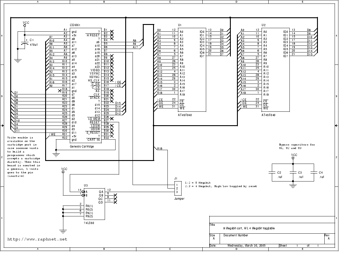
Build a reprogrammable cartridge. Many applications or games can be developed and tested on actual hardware rather than using an emulator. For those interested in Genesis development, the technical documentation available at Zophar serves as a valuable starting point....
Complex programmable logic devices (CPLDs) contain the building blocks for hundreds of 7400-series logic ICs. Complete circuits can be designed on a PC and then uploaded to a CPLD for instant implementation. CPLDs are integrated circuits that provide a versatile...
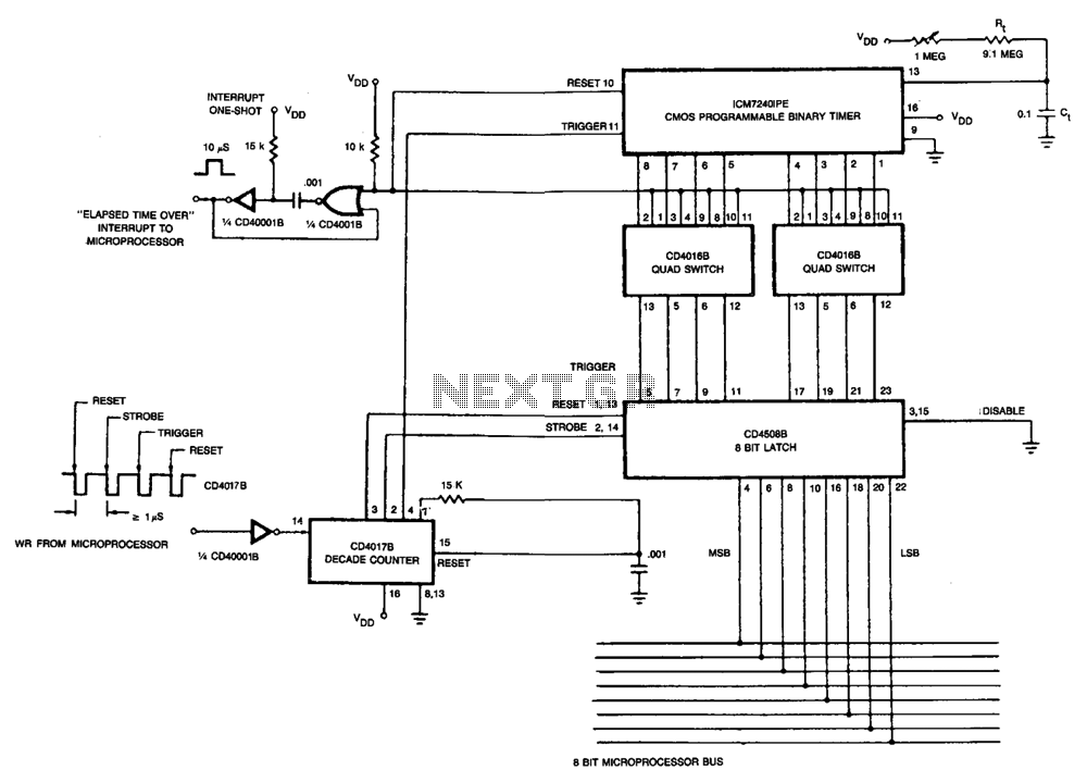
The microprocessor transmits an 8-bit binary code through its 8-bit I/O bus, which is necessary for programming the ICM7240. This is followed by four WRITE pulses directed to the CD4017B decade counter. The first pulse resets the 8-bit latch,...
I have had this project hanging around for ages and have tried to submit it for publication without much enthusiasm so I will make everything available here for the individual constructor. The complete Pascal source code for the compiler...
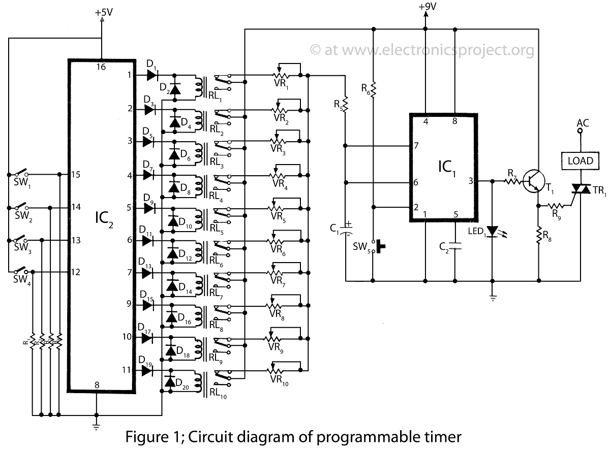
The programmable timer presented on this website is a straightforward design utilizing only two integrated circuits (ICs). It covers a wide range of applications and includes descriptions of various timer projects. The programmable timer circuit typically consists of two primary...
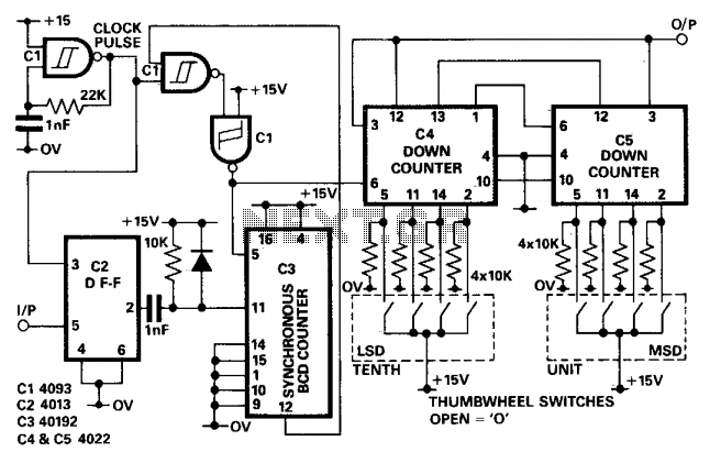
In applications where the period of the input pulses is uneven and a divider is required to accommodate a wide range of frequencies, a non-integer programmable pulse divider can be utilized. The D-type flip-flop (IC2) serves to synchronize the...