
Pulse Generator circuit

The pulse generator circuit utilizes an Atmel microcontroller, which is programmed to generate PWM signals with adjustable frequency and duty cycle. The circuit comprises a Timer1 module that is crucial for PWM generation. The output compare registers, OCR1A and OCR1C, are configured to set the duty cycle and frequency, respectively. The duty cycle is calculated based on the values in these registers, allowing for a flexible range of output characteristics.
The system clock operates at 8 MHz, and the PLL boosts the clock frequency to 64 MHz, enabling high-speed operations. The use of potentiometers allows for user-friendly adjustments of frequency and duty cycle, with the ADCs converting the analog voltage from the potentiometers into digital values that the microcontroller can process. The linear relationship of the duty cycle with respect to the output compare register values enables straightforward control, while the hyperbolic nature of frequency adjustments necessitates careful calibration for optimal performance.
The circuit includes debouncing mechanisms for the pushbuttons used to toggle the clock source and change prescaler settings, ensuring stable operation. The assembly language component of the program manages the PLL configuration, ensuring that the system can switch between clock sources without glitches. Overall, this pulse generator circuit offers a versatile solution for generating PWM signals for various laboratory applications, although it is constrained by the inherent limitations of the timer resolution and frequency scaling.A simple pulse generator with a variable duty cycle and frequency is often useful in the lab to trigger or test other devices, e. g a servo with a frequency of 50 Hz and pulses between 1 and 2 ms. This is where the project started but for reasons we see later this idea was good but just not in this case.
How is it done From the Atmel datasheet we see that the duty cycle of Timer1 is basically D = (OCR1A+1) / (OCR1C+1). The PWM frequency is fpwm = 1 / (OCR1C+1). So the duty cycle D = fpwm * (OCR1A+1). This is calculated in the Basic program. We can set the frequency and keep the duty cycle constant at e. g 50% or any other percentage when the frequency is changed. The duty cycle D scale is linear but the frequency scale is not linear, bad luck it`s hyperbolic as with most analog frequency generators, so the upper convenient frequency setting is at about 1 MHz. The frequency and duty cycle are set independently by reading 2 potentiometers with 2 ADC in a loop. The controller uses an internal 8Mhz system clock (unprogram fuse CKDIV8) and also a fast PLL clock for Timer1 at 8 times the system clock.
The PLL must be enabled and takes some time to lock, then Timer1 can run on a 64 MHz clock frequency. It takes now 1 pushbutton to toggle between PLL clock and system clock, one more pushbutton walks through the Timer1 prescaler values between 1 and 15 and back to 1 and so on.
The main program is in Basic and the part dealing with the PLL is in assembler. It`s digital and it`s 8 bit pwm so it has some granularity when you turn the potentiometers which may be a limitation or not, depends on the application. As an example, with the system clock and clock/2048 for the prescaler the Timer1 will then get one clock pulse every 512 usec, that is the limit for the resolution, in other words, the duty cycle step witdh is 512 usec in this case.
No way to get a 1 usec pulse width at a frequency of 50 Hz. 🔗 External reference
Related Circuits
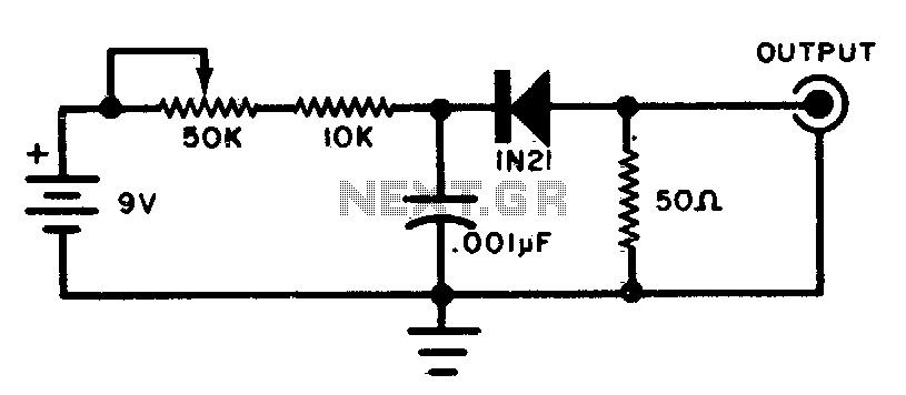
This circuit generates wideband RF noise utilizing a reverse-biased diode, featuring a low-impedance output. It can be employed to align receivers for optimal performance. The circuit primarily consists of a reverse-biased diode, which serves as the core component for generating...
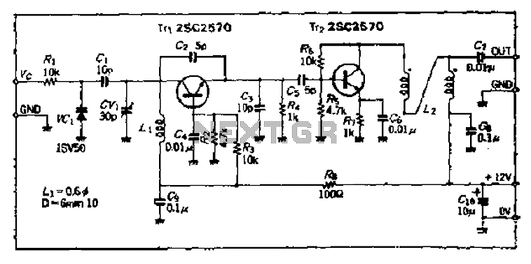
The Bong circuit is a high-frequency Colpitts oscillator that utilizes a Ge coil (L). It features two heads and is designed for simple production. The frequency of oscillation can be determined, and testing is conducted to ascertain the value...
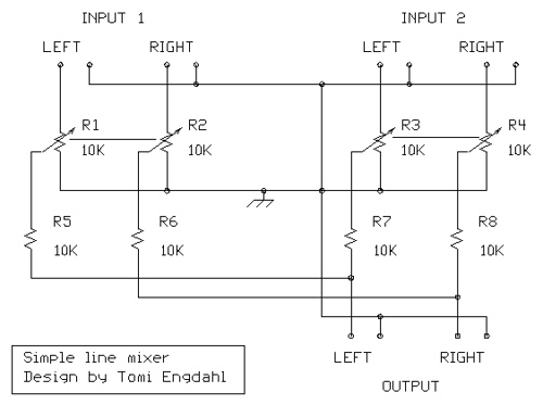
The mixer circuit described features three line inputs and three microphone inputs. The microphone inputs are designed for low impedance dynamic microphones with a range of 200 to 1000 ohms. Alternatively, an electret condenser microphone (ECM) can be used,...
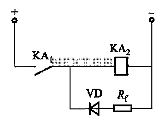
The circuit depicted in Figure 6-24 includes a relay coil with both ends connected in parallel to a resistor (Rf) or an auxiliary diode (VD). This configuration is intended to enhance power after a short circuit occurs in the...
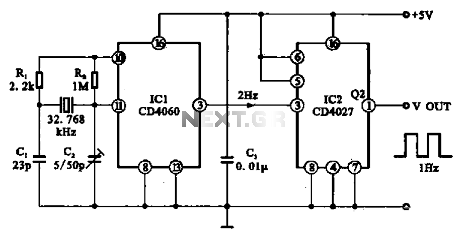
A 1Hz clock signal generator circuit is presented, which demonstrates a sophisticated clock signal generating mechanism. This circuit can be utilized for digital clocks and timing applications. It comprises a binary counter (CD4060), a JK flip-flop (CD4027), and a...
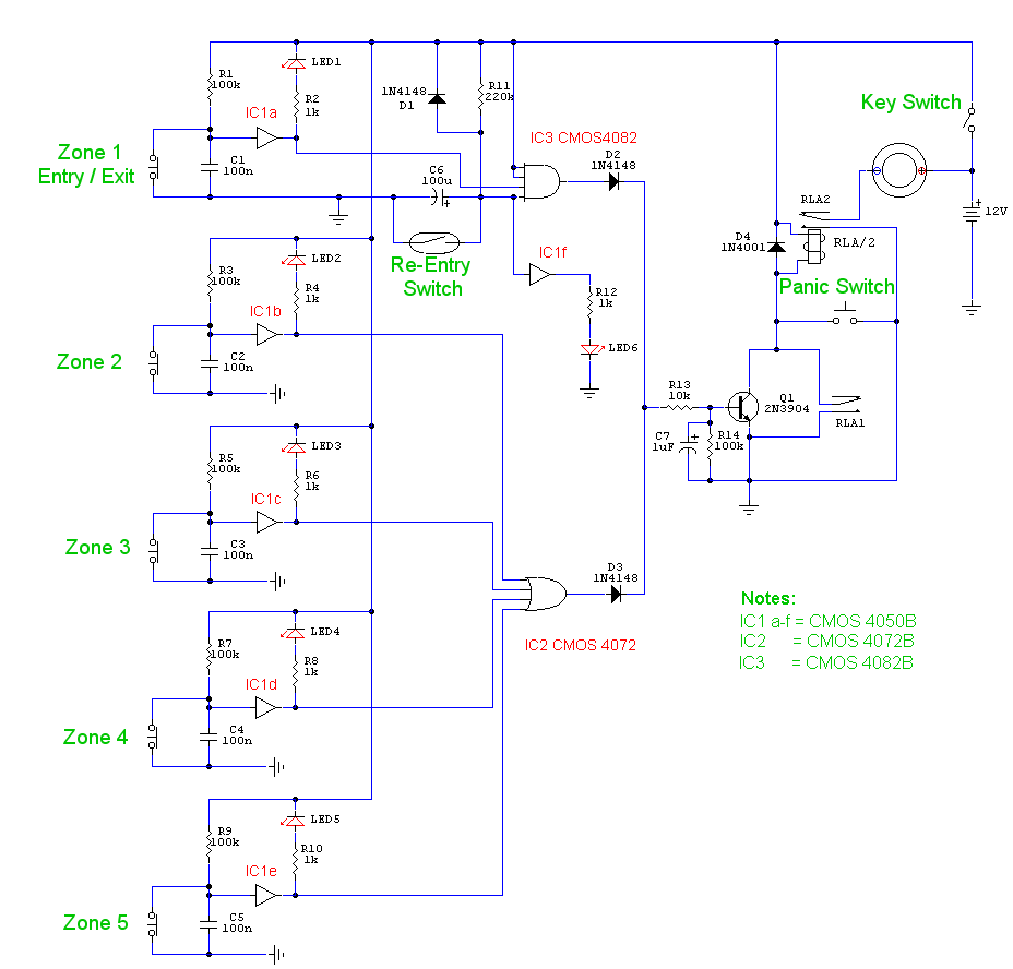
This is a complete alarm system with five independent zones suitable for a small office or home environment. It utilizes three CM integrated circuits and features a timed entry/exit zone, four immediate zones, and a panic button. There are...