
pwm lamp dimmer using ne555
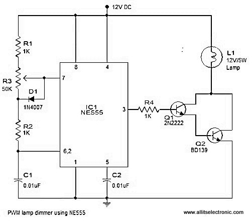
The PWM lamp dimmer circuit based on the NE555 timer effectively modulates the brightness of lamps by altering the duty cycle of the output signal. The NE555 timer, in astable mode, continuously switches between high and low states, generating a square wave output. The frequency of this output is determined by the values of R1, R2, and C1, while the duty cycle is adjusted using the potentiometer R3.
In this circuit, the NE555 timer's astable configuration allows for continuous oscillation, where the timing of the charge and discharge of capacitor C1 dictates the duration of the high and low states of the output. The use of a Darlington pair (transistors Q1 and Q2) amplifies the current to drive the lamp effectively, accommodating higher loads without overheating the components.
Diode D1 plays a crucial role in ensuring that the frequency remains stable by bypassing part of the potentiometer during the charging cycle, allowing for consistent performance across varying brightness levels. The careful selection of resistors and capacitors is essential for achieving the desired frequency and duty cycle, which directly influences the lamp's brightness.
This circuit exemplifies an efficient approach to lamp dimming, showcasing the advantages of PWM over traditional linear methods. The high efficiency of PWM dimming not only reduces energy consumption but also minimizes thermal dissipation, leading to less bulky designs and improved reliability in lighting applications. Understanding the principles behind the NE555 timer and its configuration is fundamental for engineers and hobbyists interested in developing similar projects or improving existing designs.A simple and efficient PWM lamp dimmer using timer IC NE555 is discussed in this article. Yesterdays linear regulator based dimmerscan only attain a maximum efficiency of 50% and are far inferior when compared to the PWM based dimmers which can hit well over90% efficiency. Since less amount of power is wasted as heat, the switching elements of PWM dimmers require a smaller heat sink andthis saves a lot of size and weight. In simple words, the most outstanding features of the PWM based lamp dimmers are high efficiencyand low physical size. The circuit diagram of a 12V PWM lamp dimmer is shown below. As you can see, NE555 timer IC which is wired as an astable multivibrator operating at 2. 8KHz forms the heart of this circuit. Resistors R1, R2, POT R3 and capacitor C1 are the timing components. Duty cycle of the IC`s output can be adjusted using the POT R3 higher the duty cycle means higher the lamp brightness and lower the duty cycle means lower the lamp brightness.
Diode D1 by-passes the lower half of the POT R3 during the charging cycle of the astable multivibrator. This is done in order to keep the output frequency constant irrespective of the duty cycle. Transistors Q1 and Q2 forms a darlington driver stage for the 12V lamp. Resistor R4 limits the base current of transistor Q1. As I have said earlier, the variable duty cycle astable multivibrator based on NE555 forms the foundation of this circuit and a good knowledge on it is essential for designing projects like this.
For the ease of explanation the timing side of the astable multivibrator is redrawn in the figure below. Upper and lower halves of the POT R3 are denoted as Rx and Ry respectively. Consider the output of the astable multivibrator to be high at the starting instant. Now the capacitor C1 charges through the path R1, Rx, and R2. The lower half of POT R3 ie; Ry is out of the scene because the diode D1 by-passes it. When the voltage across the capacitor reaches 2/3 Vcc, the internal upper comparator flips its output which makes the internal flip flop to toggle its output.
As a result the output of the astable multivibrator goes low. In simple words, the output of the astable multivibrator remains high until the charge across C1 becomes equal to 2/3 Vcc and here it is according to the equation Ton =0. 67(R1+Rx+R2)C1. Since the internal flip flop is set now, the capacitor starts discharging through the path R2, Ry into the discharge pin.
When the voltage across the capacitor C1 becomes 1/3 Vcc, the lower comparator flips its output and this in turn makes the internal flip flop to toggle its output again. This makes the output of the astable multivibrator high. To be simple, the output of the astable multivibrator remains low until the voltage across the capacitor C1 becomes 1/3 Vcc and it is according to the equation Toff = 0.
67(R2+Ry)C1. Have a look at the internal block diagram of NE555 timer shown below for better understanding. Whatever may be the position of POT3 knob, the total resistance across it remains the same (50K here). If anything decreases in the upper side (Rx) the same amount will be increased in the lower (Ry) and the same thing gets applied to the higher(Ton) and lower(Toff) time periods.
The derivation shown below will help you to grasp the matter easily. 🔗 External reference
Related Circuits
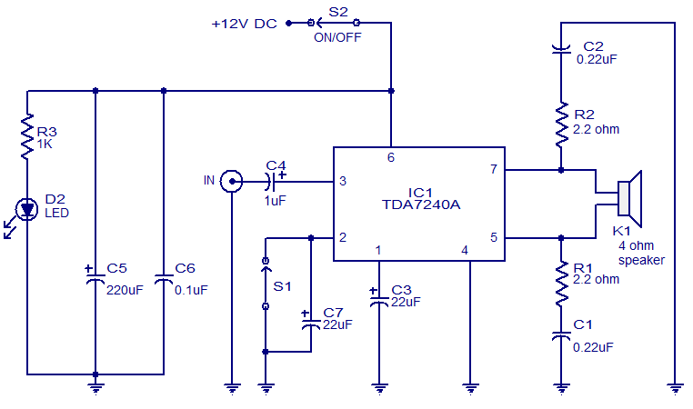
The audio amplifier presented here is based on the TDA7240 integrated circuit from ST Microelectronics. The TDA7240 is capable of delivering 20 watts of audio output power into a 4-ohm load. It requires a minimal number of external components...
A user is new to the forum and has limited experience in DIY electronics. The current project involves creating a battery-powered LED dimmer circuit. The objective of the project is to design a battery-operated LED dimmer circuit that allows for...
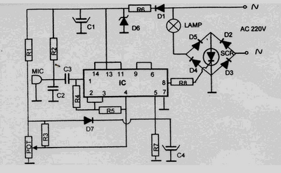
This 220 Volt disco lamp circuit is not a voice switch (VOX), as it cannot differentiate between musical sounds and human voices. Instead, it functions as a sound-activated device. An interesting application of this circuit is to control the...
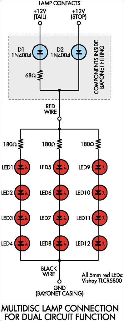
Before proceeding with the implementation, it is important to ensure that the output brightness is adequate for a stop and tail-light application. The light output may vary based on the tail-light lens and reflector assembly, so caution should be...
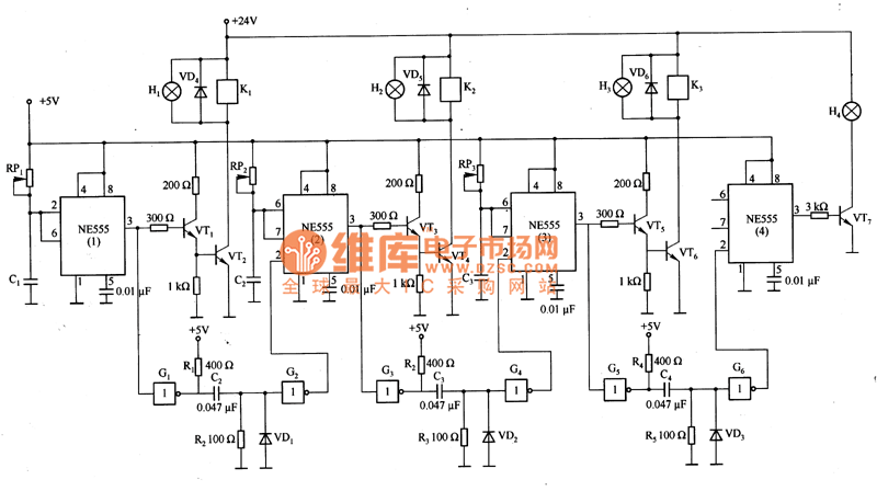
This is a sequence timer diagram composed of an NE555 timer. The timer can be set to any duration when the power is connected, allowing it to control an external system. In the circuit, K1-K3 are relays used to...
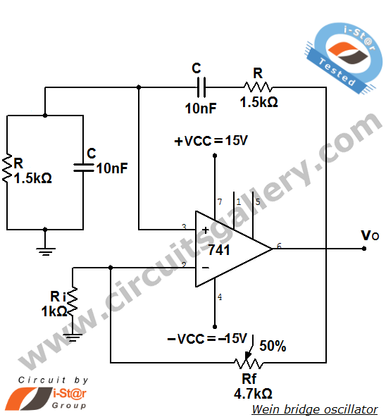
The Wien bridge oscillator is a high-stability audio frequency sine wave oscillator known for its simplicity. An oscillator is defined as a circuit that generates periodic electric signals, such as sine waves or square waves. Applications of oscillators include...
Warning: include(partials/cookie-banner.php): Failed to open stream: Permission denied in /var/www/html/nextgr/view-circuit.php on line 713
Warning: include(): Failed opening 'partials/cookie-banner.php' for inclusion (include_path='.:/usr/share/php') in /var/www/html/nextgr/view-circuit.php on line 713