
Ramp generator

The linear charging ramp circuit is essential for applications that necessitate precise voltage control over time. The architecture typically consists of a current source transistor, Q1, which is responsible for supplying a steady current to a timing capacitor, Ct. This configuration allows for the capacitor to charge in a linear manner when the timer is activated.
Upon activation, the clamp mechanism on the capacitor is disengaged, permitting Ct to charge towards the supply voltage (Vcc). The linear ramping of the voltage across Ct is dictated by the constant current provided by Q1, ensuring that the charge time is predictable and can be finely controlled.
The operational threshold for the timer is set at approximately three times the supply voltage (3 Vcc), noted as Vc. When the voltage across the timing capacitor reaches this threshold, the timing cycle is terminated, resulting in a pulse output. The output pulse width can be calculated using a specific timing expression, which is dependent on the values of the components in the circuit, including the capacitance of Ct and the current supplied by Q1.
This configuration is particularly advantageous in applications such as timers, where a precise timing interval is critical, as well as in pulse width modulation scenarios where control over the duty cycle is necessary. By adjusting the current through Q1 or the capacitance of Ct, the timing characteristics can be tailored to meet the specific requirements of the application.The linear charging ramp is most useful where linear control of voltage is required. Some possible applications are a long period voltage controlled timer, a voltage to pulse width converter, or a linear pulse width modulator. Ql is the current source transistor, supplying constant current to the timing capacitor Ct. When the timer is triggered, the clamp on Ct is removed and Ct charges linearly toward Vcc by virtue of the constant current supplied by Ql.
The threshold at pin 6 is ¥3 Vcc; here, it is termed Vc. When the voltage across Ct reaches Vc volts, the timing cycle ends. The timing expression for output pulse with is:
Related Circuits
This self-starting fixed frequency oscillator circuit provides excellent frequency stability. R1 and C1 form the frequency-determining network, while R2 supplies regenerative feedback. Diode D1 improves stability by compensating for the difference between Voh and Vsupply. In applications requiring a...
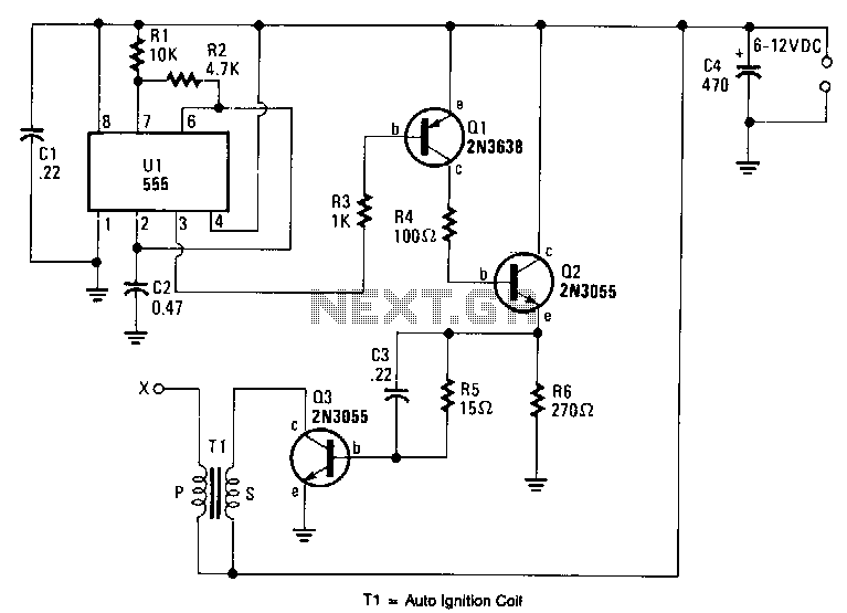
An output voltage sufficient to bridge a one-inch gap can be generated from a 12-V power source. A 555 timer integrated circuit (IC) is configured as an astable multivibrator, producing a narrow negative pulse at pin 3. This pulse...
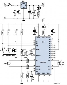
It is a common misconception that a robot voice generator box necessitates a large number of integrated circuits (ICs). In reality, the ISD2500 ChipCorder family of ICs from Winbond can effectively fulfill this requirement. The ISD2500 ChipCorder series represents a...
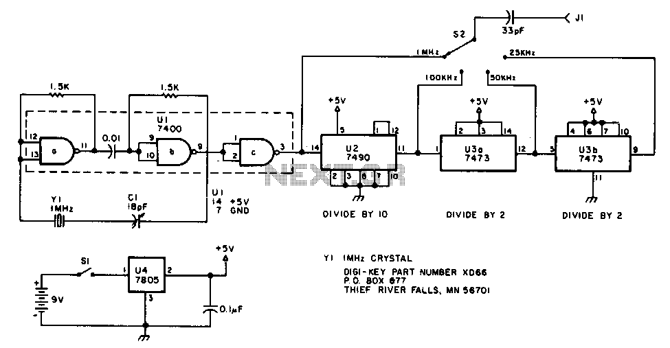
The oscillator section employs three sections of a 7400 quad NAND gate integrated circuit. The 1 MHz signal generated by the oscillator is input into a 7490 decade counter, which is configured to divide by ten, producing a 100...
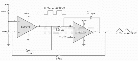
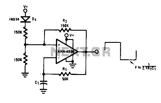
The circuit has both square-wave and triangle-wave output. The left section is similar in function to a comparator circuit that uses positive feedback for hysteresis. The inverting input is biased at one-half the Vcc voltage by resistor R4 and...
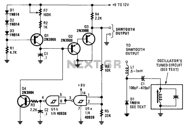
This circuit generates a linear sawtooth waveform with a frequency range from 30 Hz to 3,000 Hz. Q1 acts as a constant-current source that charges capacitor C1 until the output level at the emitter of Q3 triggers operational amplifiers...