
RC transmitter with MC68HC711


The SUPERTEF 96 represents a significant advancement over its predecessor, the SUPERTEF version utilizing the 68HC11 microprocessor. The transition to the 68HC711E9 microprocessor, which features an internal program memory and operates in "mono-chip" mode, markedly simplifies the design by eliminating the need for multiple external integrated circuits (ICs). The internal memory capacity of 12 Kbytes enhances program performance compared to the previous model's 8 Kbytes, while a small external memory is incorporated to support data storage for up to 27 models.
The analog section of the coder, as depicted in Figure 1, includes four operational amplifiers (U3) responsible for processing the stick voltages (v1 to v4) with adjustable gains via potentiometers P1 to P4, and neutral fine adjustments through P5 to P8. The output voltages (ranging from 0 to +5V) are directed to the microprocessor. Auxiliary signals (v5, v6, v7), trim adjustments (TR1 to TR4), and the gas channel voltage (v4) are multiplexed by U1 and U2 in synchronization with the input signal before being transmitted to the microprocessor's peripheral inputs (PE3 to PE7).
The design recommends the use of an LM660 operational amplifier for U3, providing an output range compatible with the A/D converter of the microprocessor. Reference levels VRL and VRH can be configured to 0V and +5V, respectively, achieved by setting resistor values R12 and R13 to zero, although alternatives such as the MC14573 with additional resistors can be utilized.
Amplifiers U4A and U4B are dedicated to processing signals for the frequency synthesis module and formatting the PPM signal, respectively. The microprocessor's Port E serves as the 8-bit A/D converter, allowing for a resolution of 256 discrete levels, which translates to an angular precision of approximately 0.3 degrees for standard servo movements.
Port B is designated for a 2x16 character LCD display, while Port C manages keyboard inputs and function switches. Port A handles various outputs, including signal output, HF module recognition, and tachometer functions, with Port D facilitating communication with peripherals such as model memory (U6), the frequency synthesis module, and RS232 connections for interfacing with other SUPERTEF units or PCs.
A reset circuit (U7) ensures proper initialization of the microprocessor at power-up, and a protective diode (D18) safeguards against voltage spikes. The principal printed circuit board (T board) consolidates the connections for the continuous voltage from sticks, trims, and auxiliaries, and accommodates dual-rate buttons and mixing controls. It also hosts power regulation circuits providing 5V and 10V outputs and facilitates keyboard signal transmission through designated connectors (CONN3 to CONN6).
The keyboard and associated components are illustrated in Figure 4, featuring input buttons and a buzzer control transistor, with connections to the T board and additional accessories. This streamlined architecture enhances reliability and reduces the risk of defects inherent in densely populated circuit designs.The first SUPERTEF version was using a 68HC11 microprocessor in extended mode i.e. with an external memory program which necessitated many integrated circuits (IC) such as the 74C138, 74C373, 68HC24 and 27C64 making the printed circuit board densely populated and prone to defects. Now, SUPERTEF 96 uses a 68HC711E9 that is to say the same basic chip but with an INTERNAL program memory operating in "mono-chip" mode without the need for all the IC's above.
The coder then became ultra-simple and except for monstrous errors, cannot not function since all that is active is IN the microprocessor. The INTERNAL storage in question has a capacity of 12 Kbytes instead of the 27C64's 8 Kbytes. The program is more performant. Let us say that it was necessary all the same to add a small external memory storage to place the data for 27 possible models.
Figure 1 shows the diagram of the analog part of the coder. You see on the left the 4 amplifiers (U3) of the sticks' voltage (v1 to v4) with adjustment of the gains using P1 to P4 and the neutral fine adjustments, using P5 through P8. The outputs (0 to +5V) P0 to P2 are sent directly to the microprocessor. On the other hand, the auxilliaries (v5, v6 and v7), the trims (TR1 to TR4) and the gas channel (v4) are multiplexed by U1 and U2 in synchrony with the signal, before being transmitted to the microprocessor (PE3 to PE7).
The circuit U3 should preferably be a LM660 from NS, with an output of 0 to +5V. Under these conditions, one can make VRL=0V and VRH=+5V, (they are the levels of reference of the A/D converter of the 68HC711) which is obtained with R12 = R13 =0. However the printed circuit makes it possible still to use a MC14573 with R12 = R13 = 47 ohms and the addition of R18.
The amplifier U4A leads the tension of VARICAP of the frequency synthesized HF module and thus allows an alarm if the range of authorized variation is exceeded. The amplifier U4B formats the PPM signal by giving it the amplitude of 8V DC and the tilted sides necessary to obtain a correct HF spectrum figure.
Fig. 2 illustrates the superb simplicity of the coder logic: U5 and... that is all! Port E is the 8-bit A/D converter of the microprocessor. Note that with 8 bits, it is possible to define 256 levels of precision. Knowing that a servo normally turns only 90 degrees, that gives us an accuracy of 90/256 = 0.3 degree approximately. So when we read in advertisements for instance that "... demanding pilots need an accuracy of 10 bits .) that is to say 1024 levels, each one 0.08ø (yes, 8 hundredths of a degree!) we...
laugh, quite simply! Port B manages the LCD display of 2x16 characters. Port C manages the keyboard and all the function switches. Port A has various missions: signal output, recognition of the type of HF module inserted, tachometer, buzzer.. Finally port D ensures the communication with the peripherals: model memories (U6), frequency synthesis HF module and an RS232 connection to another SUPERTEF or to a PC.
The small circuit U7 ensures a correct reset of the microprocessor at power up, while the diode D18 protects all this small world from excessive voltage. Figure 3 represents all the connections ensured by the principal printed circuit board (referred as the T board because of its T-shape).
This PCB collects the continuous voltage of the sticks, trims and auxilliaries. It hosts the dual-rate buttons DR1 to DR3, and those mixing CP1 to CP3 on channel 8. Lastly, the T board hosts the power circuits and the 5V and 10V regulators. Also, the T board conveys the signals PC0 to PC7 going to the keyboard, through connectors CONN3 to CONN6, but also necessary for all other functions of the board itself. Figure 4 is the diagram of the keyboard and appendices. One finds there the 4 keyboard input buttons, P, E - and +, the transistor commanding the buzzer, connectors CONN7 to CONN9 linking with the T board and the accessories located on the right side of the transmitter.
🔗 External reference
Related Circuits
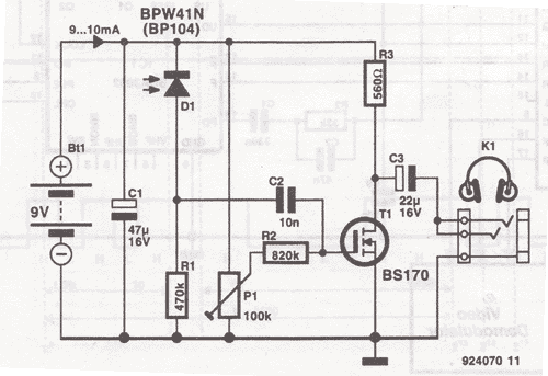
This wireless headphones transmitter ensures quality reception over a distance of 2 meters. The oscillator frequency ranges from 1750 kHz to 3500 kHz, and for the antenna, it... The wireless headphones transmitter operates within a frequency range of 1750 kHz...
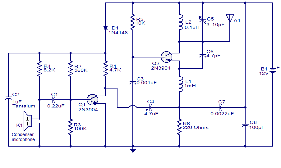
The FM transmitter circuit presented is both stable and simple. With an adaptive antenna, it can achieve a transmission range of approximately 200 meters. This transmitter was developed this year and has yielded positive results. The circuit operates using...
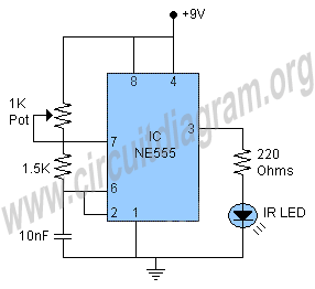
This schematic illustrates an infrared (IR) transmitter circuit utilizing an integrated circuit (IC). The circuit employs the widely recognized NE555 timer IC, which operates as an astable multivibrator to generate a signal with a frequency of 38 kHz. The...
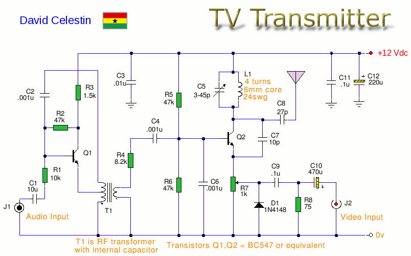
This is an analog TV transmitter. Sound modulation is of the FM type with a 5.5 MHz carrier frequency, and video transmission follows the PAL standard. The frequency can be adjusted using capacitor C5, allowing tuning from 54 to...
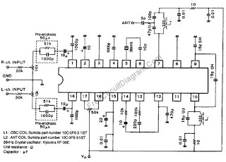
This wireless stereo FM transmitter is constructed using a monolithic integrated circuit (IC). The internal architecture of this FM transmitter IC includes a stereo modulator that generates a stereo composite signal, an FM modulator that modulates a carrier frequency...
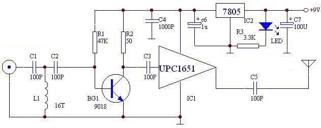
The UPC1651 FM monolithic circuit can be utilized to design a simple, low-cost FM transmitter electronic project. This circuit is specifically designed as a wideband amplifier that covers the HF band through the UHF band. Audio signals from the...