
Reflex Radio Receiver
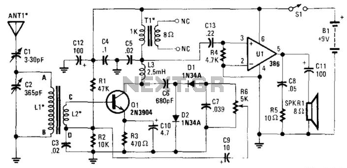
The circuit operates by first capturing the RF signal through the antenna, which is then processed by CI. The tuned circuit, composed of inductor LI and capacitor C2, is essential for filtering and selecting the desired RF frequency. The configuration of L2 plays a crucial role in coupling the RF signal to the base of transistor Q1, ensuring that the transistor receives the necessary bias from the resistor network formed by R1 and R2. The use of capacitor C3 at RF ground prevents unwanted RF signals from affecting the circuit's operation.
Following amplification by Q1, the RF signal is further processed by capacitor C6, which allows the signal to pass while blocking DC components, directing it to the rectifier circuit. The two-diode doubler/rectifier circuit converts the RF signal into a usable audio signal, which is then adjusted by the volume control, R6. The output from R6 is connected to capacitor C9, which serves to couple the audio signal to the junction of R1, R2, and the "D" end of L2.
The unique grounding arrangement ensures that the "D" end of L2 is at RF ground, allowing the audio frequency (AF) signal to pass through to the base of Q1 without interference from RF components. The choke, rated at 2.5 mH, along with transformer T1, is strategically placed at RF ground through capacitor C5 to maintain signal integrity.
Finally, the amplified audio signal is fed into the 386 audio amplifier, U1, which is capable of driving an 8-ohm speaker. This configuration highlights the versatility of the transistor, which serves to amplify both RF signals for reception and AM signals for audio output, demonstrating an efficient design for radio frequency applications. The RF signal is passed from the antenna through CI to the tuned circuit made up of LI and C2. One end of L2 feeds th e RF signal to the base of Ql for amplification and the other end ties to the junction of Rl and R2 to supply bias to the transistor. A 0.02-/xF capacitor, C3, places the "D" end of LI at RF ground. The amplified RF signal is fed through C6 to a two-diode doubler/rectifier circuit and then on to the volume control, R6.
The wiper of R6 feeds the detected audio signal through C9 to the junction of Rl, R2, and the "D" end of L2. The "D" end of L2 is at RF ground, but not AF ground, allowing the AF signal to be passed through L2 to the base of Ql for amplification.
The junction of the 2.5-mH choke and Tl is placed at RF ground through C5. The amplified audio is fed from this junction to the input of the 386 audio amplifier, Ul, to drive the 4" 8- speaker. The single transistor has performed a dual duty by amplifying the RF and AM signals at the same time.
🔗 External reference
Related Circuits
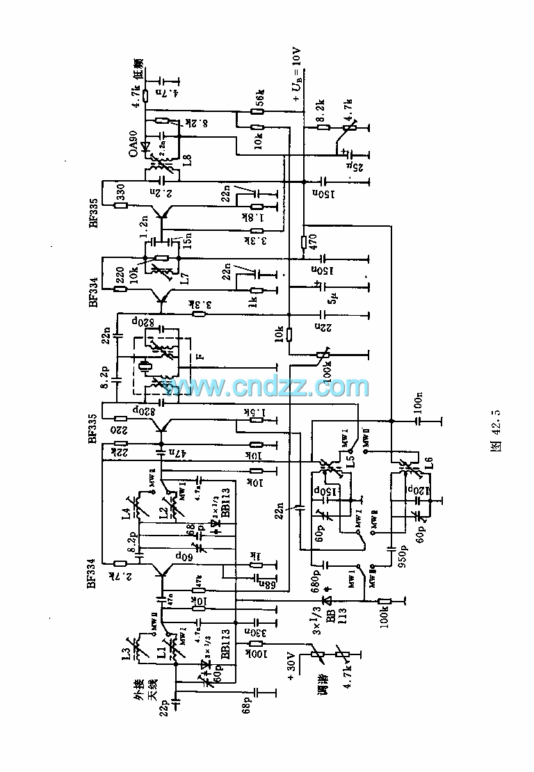
This circuit illustrates the high and mid-frequency sections of a car radio. The medium wave band I operates within the frequency range of 520 to 950 kHz, while Poland II operates between 900 and 1640 kHz. The circuit employs...
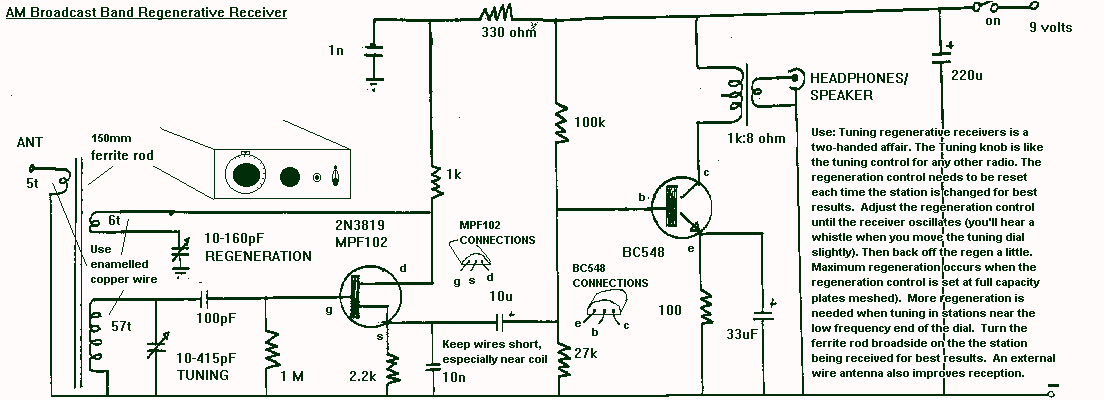
The regenerative detector uses a field effect transistor (FET). Like with the better valve designs, feedback is controlled by a variable capacitor. A ferrite rod was used to allow reception of local stations without an external antenna. This FET...

A radio camera on a model railway should transmit constantly while the train is moving and continue transmitting for a few minutes after the train stops. The design of a radio camera system for a model railway requires careful consideration...

An AM radio can be constructed using a simple diode detector and an audio amplifier. A random length of wire typically serves as an antenna. LI is an adjustable ferrite loopstick similar to those used in transistor radios. An AM...
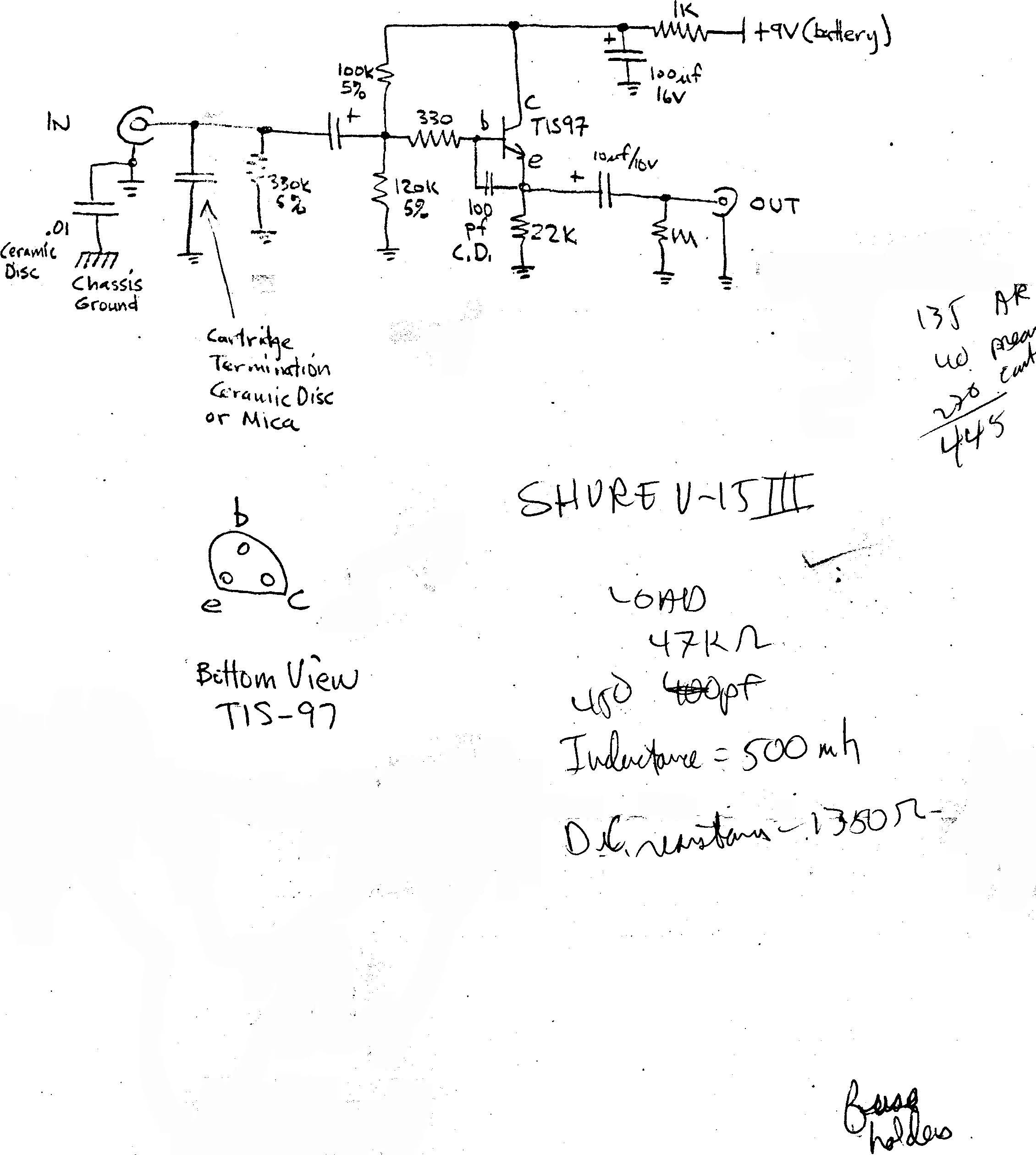
The infrasonic filter was a particularly useful feature of the phono preamp. Instructions were provided on how to build an external buffer circuit to use with any phono preamp, in order to avoid cartridge impedance interaction. A letter was...
The TPTG transmitter has been transformed into a modern TNT model. This transmitter can utilize the existing K-111 power pack for both the transmitter and receiver, eliminating the need for a separate power supply unit. Building this compact transmitter...