
Removable Memory Card (MMC) on mobile phones circuit

The memory card circuit in mobile phones is a critical component that facilitates data storage and retrieval. The circuit typically comprises several key elements, including the memory card itself, the application processor, and various filtering components. The memory card can operate in two modes: Secure Digital (SD) mode and Serial Peripheral Interface (SPI) mode. In SD mode, the memory card utilizes all its pins for communication, ensuring a high-speed data transfer rate and efficient operation. This mode is commonly used for standard SD cards, miniSD cards, and microSD cards.
In contrast, SPI mode restricts the use of certain pins, which can simplify the circuit design and reduce power consumption. However, this mode typically offers slower data transfer rates compared to SD mode. The choice between these modes depends on the specific application and the requirements of the mobile device.
The block diagram serves as a visual representation of the memory card's integration within the mobile phone's architecture. It highlights the connection pathways between the memory card and the application processor, which is responsible for managing data operations. Additionally, the diagram illustrates the presence of ESD and EMI filtering components, which are essential for maintaining signal integrity and protecting the circuit from external disturbances. These filters are strategically placed to shield sensitive components from potential damage caused by electrostatic discharge and electromagnetic interference.
Understanding the schematic diagram is vital for technicians and engineers involved in troubleshooting memory card issues. By analyzing the connections and identifying whether the circuit is designed for SD or SPI operation, one can effectively diagnose and repair problems related to memory card functionality. This knowledge is indispensable for ensuring the reliability and performance of mobile devices.In this tutorials we are going to tackle out how dos the memory card circuit works on mobile phones. As in my previous post I talked about memory card pin-outs and types of memory cards used on cellular phones. Okay, the block diagram below shows how the removable memory card or MMC card connection to other corresponding components.
Since the mem ory card has two signal function operations, the SD mode and SPI mode, the SD mode indicates that all pins of the memory card ether SD card, miniSD card and microSD card has a connections while in SPI mode some of the pins are not connected. See the block diagram below. In mobile phones ESD and EMI filtering were so very important, the connection between the memory card across to the application processor is being filtered or protected by any means of ESD and EMI interruption.
The best easy way to identify which one has SD or SPI designed, is by figuring it out on the schematic diagram, and it is so important to know about this for easy troubleshooting and repair memory card related problem issues. 🔗 External reference
Related Circuits
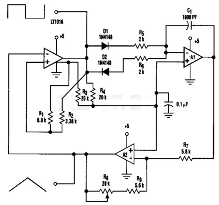
This function generator, based on an LT1016 high-speed comparator, will generate from a single +5-V supply. The slow rate of the op-amps used determines the maximum usable frequency of this circuit. The function generator utilizes the LT1016 high-speed comparator to...
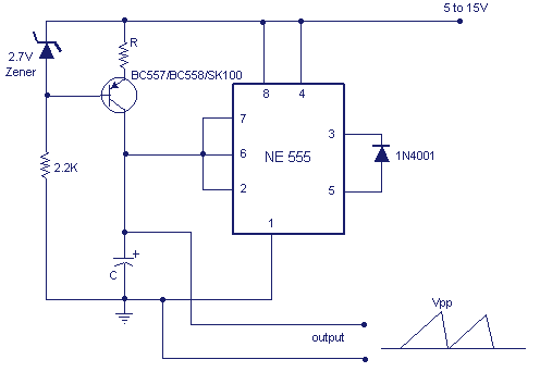
A sawtooth wave generator circuit using a 555 IC is presented in the article below. The frequency equation is provided with the supply voltage Vcc. The sawtooth wave generator circuit utilizing a 555 timer integrated circuit (IC) is a fundamental...
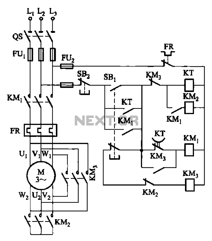
The circuit depicted in Figure 3-41 illustrates a Y-transfer process. When contact KMi is turned off, the motor undergoes a transition in the event of a power failure. Additionally, the main contact KM3 is disconnected when KM2 is activated,...
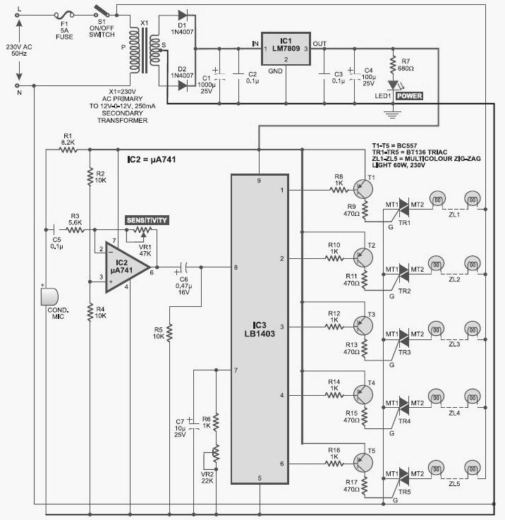
This light chaser circuit, which functions as a music-operated lighting effect generator, consists of five sets of 60W bulbs arranged in a zig-zag configuration. The light chaser circuit is designed to create dynamic lighting effects that synchronize with music, enhancing...
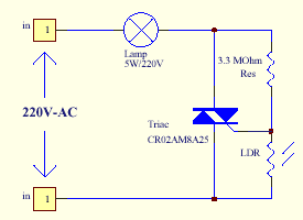
The series of light switches is slightly different from traditional designs. These light switches can operate directly on the AC power network. The main components of the circuit include a TRIAC and a Light Dependent Resistor (LDR). The circuit...
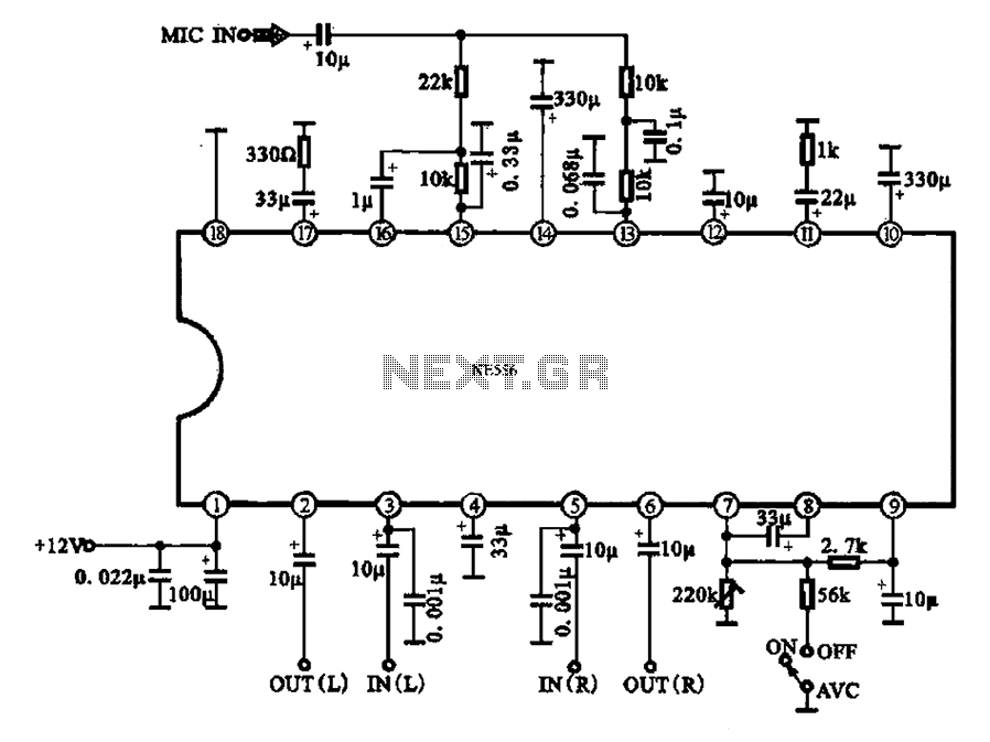
Automatic volume adjustment with ambient noise control circuit. In car stereos and similar devices, the ambient noise level varies during high-speed and low-speed driving or while stationary, leading to different volume requirements. A fixed volume adjustment method may negatively...
Warning: include(partials/cookie-banner.php): Failed to open stream: Permission denied in /var/www/html/nextgr/view-circuit.php on line 713
Warning: include(): Failed opening 'partials/cookie-banner.php' for inclusion (include_path='.:/usr/share/php') in /var/www/html/nextgr/view-circuit.php on line 713