
RF transmitter uses AMI encoding

The described circuit is a sophisticated 16-channel RF transmitter designed for efficient data transmission in the unlicensed ISM band. It operates at data rates up to 28.8 kbps and is capable of maintaining reliable communication over distances up to 1000 feet in open-field conditions. The core functionality relies on the AMI encoding process, facilitated by integrated circuits IC1 and IC2. The D flip-flop configuration in IC1A ensures controlled high-impedance states, while IC1B manages data transitions to prevent output glitches.
Resistors R1 and R2 play critical roles in establishing a stable high-impedance voltage at half the supply voltage, which is essential for proper signal integrity. The modulation characteristics of the RF signal are fine-tuned through the varactor diodes D1 and D2, with D1 providing modulation control and D2 setting the center frequency. The output power of the transmitter can be adjusted via resistor R3, allowing for flexibility in different operational environments.
The circuit employs a lowpass filter configuration using capacitors and inductors (C2/L1 and C3/L2) to ensure impedance matching between the transmitter and the load, which is vital for minimizing signal reflections and maximizing transmission efficiency. Final output filtering is achieved with component CF1, which is crucial for maintaining signal purity before transmission.
Frequency synthesis is accomplished through IC4, which uses a crystal oscillator to derive the desired carrier frequency. The internal division by 512 allows for precise frequency control across the defined channel range. The resulting output channels span from 902.72 to 906.62 MHz, with a step size of 260 kHz, providing a robust selection of channels for various applications.
Careful attention to the layout and shielding of the circuit is advised to mitigate interference and enhance performance. Additionally, implementing decoupling measures will improve the stability of the power supply across the circuit components. For low-power applications, the option to disable the transmitter by holding Pin 17 of IC3 at logic zero further enhances the versatility of this RF transmitter design.The circuit in Figure 2 shows a 16-channel, AMI-encoded RF transmitter for data rates as high as 28.8 kbps. The circuit operates in the unlicensed (FCC Part 15) 902- to 928-MHz industrial, scientific, and medical (ISM) band and is reliable for open-field distances as long as 1000 ft.
You can easily modify it to sustain higher or lower data rates. IC1, IC2, R1, and R2 perform the AMI encoding. IC1A, a simple D flip-flop, controls the high-impedance state on Pin 13 of IC2. IC1B alternates the data presented to IC2 whenever the previous data is a logic one. This data has a slight delay to avoid glitches in the output waveform. R1 and R2 set the high-impedance voltage to ½VCC. R2 adjusts the peak deviation of the transmitted RF signal from IC3, nominally set at 50 kHz. C1 and R2 constitute a lowpass filter with corner frequency set to attenuate the data at frequencies above the third harmonic.
IC3 is a low-power, integrated RF transmitter (Motorola, www.motorola.com) targeting ISM applications. Its voltage-controlled oscillator is a parallel-resonant Colpitts type. The varactor diode, D1, controls the modulation, and D2 sets the center frequency. The modulation, D1, is set to approximately 60 kHz/V, and the frequency adjustment, D2, is set to 7 MHz/V.
The mixer of the IC serves as a buffer; you can adjust R3 for desired output power. C2/L1 and C3/L2 conjugately match the source-to-load impedances. These values can vary, depending on the parasitics of your layout. CF1 (TDK Corp, www.tdk.com) provides final filtering of the output before transmission. IC4 synthesizes the desired carrier frequency. The IC internally divides by 512 the frequency that crystal Y1 establishes. With Pin 16 of IC3 tied low, the synthesized frequency is fOUT=(2.048 MHz/512)*65*N, where N represents the digital value present on the N bus of IC. As illustrated, N can vary from 3472 to 3487, yielding 16 discrete output channels from 902.72 to 906.62 MHz in 260-kHz steps.
R4 and C4 form a lowpass filter with corner frequency set to a value substantially lower than the internal reference frequency of the synthesizer or the data stream, whichever is lower. As with any RF design, you should give careful consideration to parts placement and shielding. You should also apply generous decoupling. If desired, you can hold Pin 17 of IC3 at logic zero for low-power-disabled operation.
Related Circuits
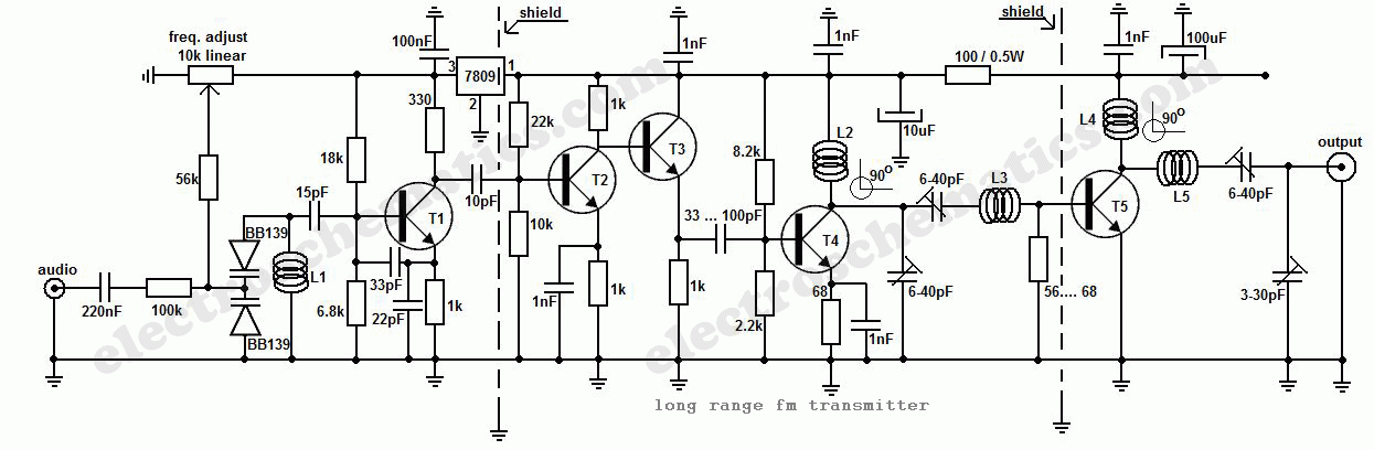
This circuit is a highly stable, harmonic-free, long-range FM transmitter designed to operate within FM frequencies between 88 and 108 MHz. It is capable of covering a range of up to 5 kilometers. The circuit features a stable oscillator...
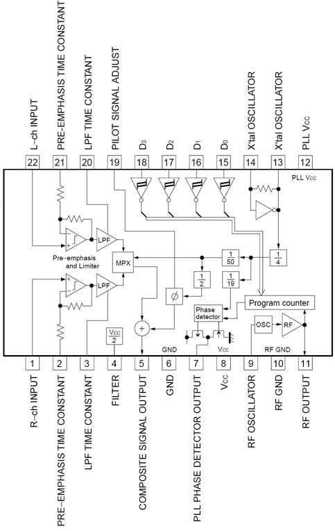
The BH1417 FM Transmitter architecture from RHOM is a compact solution that integrates multiple features into a single package. It includes pre-emphasis and a limiter to ensure that music is transmitted at the desired audio level, as well as...
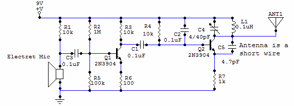
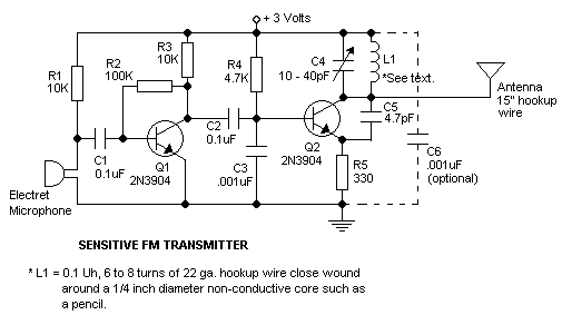
This circuit uses a small microphone to capture the sound and some transistors to generate radio waves that can be picked up by a FM receiver like a car stereo. The first part is the microphone and some resistors...
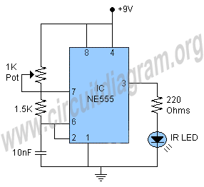
This schematic illustrates an infrared (IR) transmitter circuit utilizing an integrated circuit (IC). The circuit employs the widely recognized NE555 timer IC, which operates as an astable multivibrator to generate a signal with a frequency of 38 kHz. The...
This is an image Schematic. No Description available. The provided input indicates that there is an image schematic without a detailed description available. In typical electronic schematics, various components such as resistors, capacitors, diodes, transistors, and integrated circuits are...

This is a design circuit for a UHF transmitter. The TV transmitter operates within the UHF frequency range of 470-580 MHz, specifically on channels 21-34. It can transmit signals over distances of 30-100 meters using a cable length of...