
ring generator circuit
Historically, during the 1960s and 1970s, telephone exchanges generated ringing (as well as busy and disconnected signals) using mechanical systems like micro switches actuated by sector discs on a constant-speed motor shaft. Current designs available online vary widely, with some employing unsafe methods such as feeding raw 110V AC into the phone, while others use oscillators connected to audio amplifiers or complex electronic devices with high component counts. A low DC voltage (15V) is typically sourced through a plug pack using conventional methods like bridge rectifiers, filter capacitors, and three-terminal regulators.
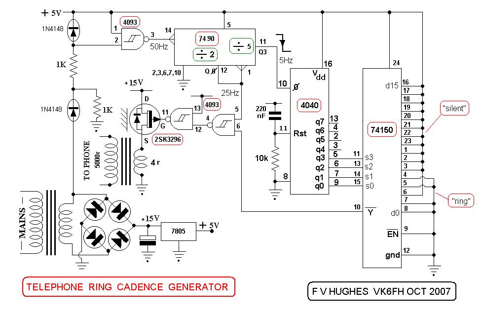
This design samples low voltage AC from a transformer secondary through a diode to create a unidirectional 50 Hz signal that serves as a clock. The positive half-wave sinusoidal signal is fed into a 4093 Schmitt trigger, which generates a fast rise and fall square wave necessary for clocking subsequent logic ICs. A clamping diode between the Schmitt trigger input (pin 2) and the Vcc rail prevents the input voltage from exceeding one diode drop above Vcc, with excess voltage dissipated across a 1K resistor. The cleaned-up 50 Hz clock signal is then directed to a 7490 counter, which divides the frequency by 2 to yield 25 Hz (the ringing frequency) and further divides by 5 to produce a 5 Hz signal, corresponding to a 200 ms interval suitable for the desired ringing cadence.
The sequential outputs of the 4040 counter connect to the address lines of a 74150 multiplexer, which switches between 16 inputs to produce the correct cadence for the ringing signal. Gating is accomplished using a 4093 NAND gate, whose output directly drives the gate of a VMOS FET, which switches the unregulated 15V rail onto the primary of the transformer. The VMOS FET is preferred over bipolar transistors due to its superior power handling capacity and low on-state resistance, ensuring minimal voltage loss across the device. These FETs also feature an internal reverse-biased diode between the drain and source, providing protection against transient spikes. The specified FET model, 2SK3296, can be salvaged from defunct computer motherboards, though suitable replacements are readily available.
A loudspeaker transformer with a 5000-ohm to 4-ohm impedance ratio is utilized in reverse to step up the voltage to the level necessary to actuate the bell solenoid (with a 1:35 ratio). In conclusion, the constructed and tested design operates effectively, producing a ringing sound reminiscent of traditional telephones.Restore the older style of telephones which used a pair of gongs to annunciate an incoming call, AND long to hear the nostalgic peel of those bells Presented here is a design for a "Telephone Ring Generator" which when connected to a suitable telephone will cause the bells to ring in the correct "cadence"- for what I might call the "British Post Office" type format. (in common use in many parts of the world) 400mS ring, 200mS silence, 400mS ring followed by 2 second silence (3 second total - then cycle repeats) The ringing frequency of the bells is reckoned to be about 25Hz The ringing sequence used in the USA is 4 secs ring, 8 secs silent, 30Hz ringing frequency, then cycle repeated. The design could in fact be "re-hashed" to deliver this format, a later update may follow. From my own recollection of telephone exchanges c1960/70`s the ringing (and also busy and disconnected ) signals were generated by micro switches actuated by sectored discs all rotating on the shaft of a constant speed motor !
Whilst there are designs and ideas on the internet that try to achieve the above; they range from feeding raw 110v mains AC into the phone (crude and dangerous!), oscillator into audio amplifier feeding the phone (may work but somewhat messy), to electronic devices using free running RC oscillators and a lot of associated components (high parts count). A plug pack or similar is used to obtain a low DC voltage (15v) to power the electronics - by conventional means; bridge rectifier, filter capacitor, 3 terminal regulator etc.
Nothing new here. Additionally low voltage AC from the transformer secondary is sampled through a diode to provide a unidirectional 50Hz signal which can be used as a "clock" This positive going half-wave sinusoid is fed to a 4093 Schmitt trigger, its action being to produce a fast rise (and fall) square wave necessary to clock following logic IC`s. A clamping diode b/w the Schmitt input (pin 2) and the Vcc rail precludes the input from rising greater than one diode drop above Vcc, excess voltage being dropped across 1K resistor.
This cleaned-up 50Hz "clock" signal is now fed to a 7490 where divide by 2 gives 25Hz (for ringing frequency) and further divide by 5 give 5Hz or a 200mS interval suitable for producing the correct ring cadence. The sequential outputs of the 4040 are connected to the address lines of a 74150, being a 1 of 16 "multi-plexer" Each of 16 inputs is sequentially switched (in inverted form) thru to the output.
The 16 inputs are hard wired to Vcc or Gnd as necessary to give the correct cadence (as stated above) for the ringing signal. Gating is achieved in the 4093 NAND gate, its output then inverted directly feeds a VMOS FET gate which switches the unregulated 15v rail onto the transformer primary.
I preferred a VMOS FET over a bipolar transistor etc here because of their power handling capacity and very low "on" state resistance (milliohms) which allows most of the +15v DC rail be available to the transformer winding. Fortunately these devices also have an internal reversed biased diode, b/w drain and source which protects them against failure from transient spikes (refer to manuf` data sheets).
The particular FET specified 2SK3296, I salvaged several from defunct P4 computer mother board (in power supply circuit). However suitable replacement types are easily available. I have used a 5000 ohm to 4 ohm loud-speaker transformer (in reverse - so to speak) to step up the voltage to the level necessary the make the bell solenoid actuate the armature (1 : 35 ratio) In summing up, I have constructed and tested the above design and find it works well, and the telephone ( ring ) is just as you might remember it !
🔗 External reference
Related Circuits

Each bistable circuit comprises two oppositely-symmetrical germanium transistors, two diodes, and four resistors. An additional transistor, Q, facilitates the transition of the conducting state to the next position when actuated by a transfer pulse. The absence of capacitors allows...
This circuit generates a stable 1 kHz sine wave using an inverted Wien bridge configuration composed of components C1, R3, C2, and R4. It features a variable output, low distortion, and low output impedance to ensure good overload capability....
A logic pen, also known as a logic detection probe, is a commonly used tool for detecting the logic state at various points within digital circuits. The logic states in digital circuits are typically categorized into three types: a...
By adjusting the oscillators so their frequencies are very nearly the same, the difference between them is made audible as a beat note. This beat note changes slightly when the search loop is moved over or near to a...
This is a simple circuit that features high-performance power amplifiers. The power amplifier is available as a PCB, along with a complete list of components. The described circuit utilizes high-performance power amplifiers, which are essential for applications requiring significant signal...
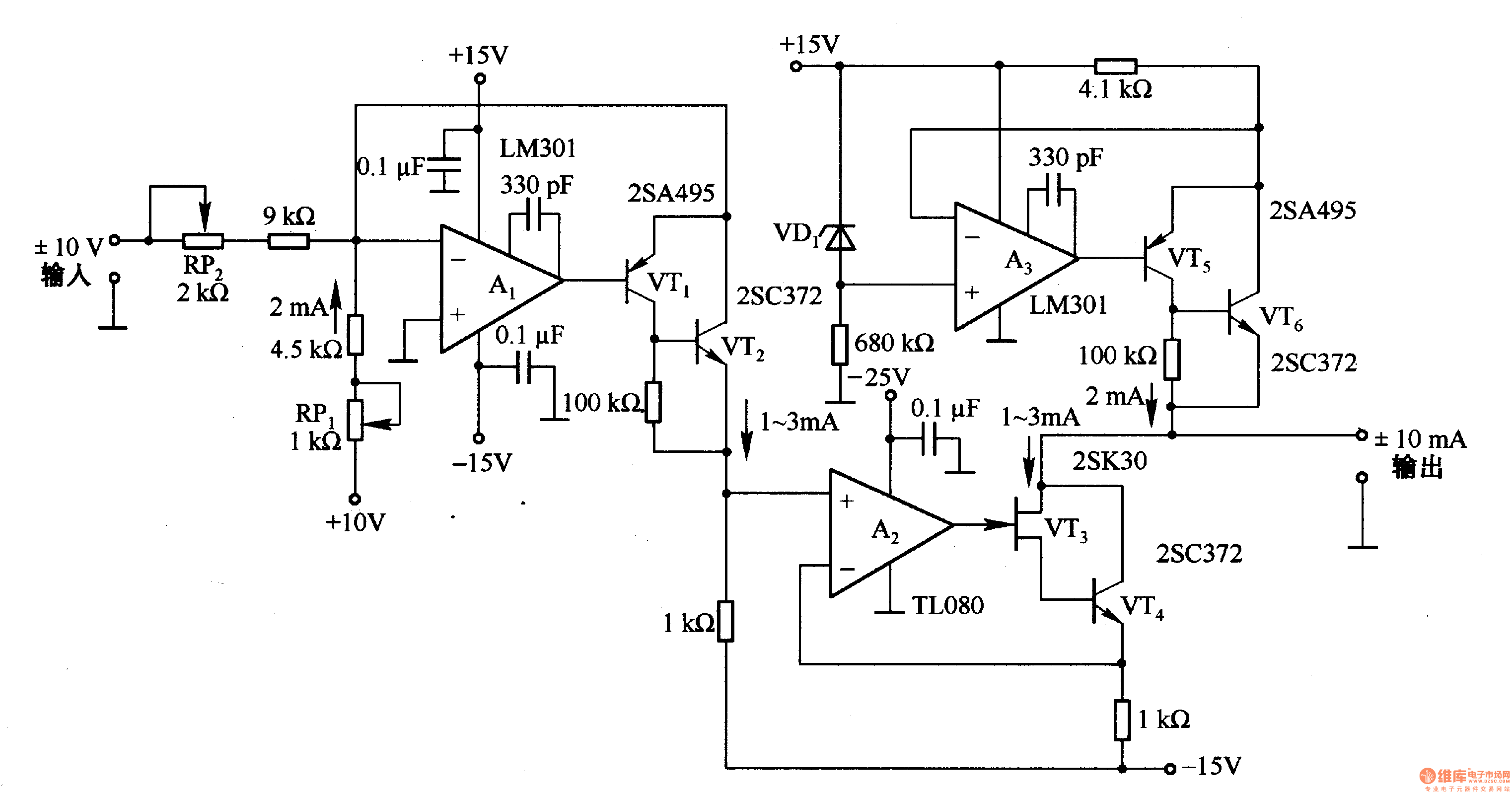
This circuit is designed for voltage-to-current conversion, specifically transforming a ±10V input voltage into a ±1mA output current. The conversion process is facilitated by operational amplifier A1 and transistors VT1 and VT2, which are responsible for altering the current...
Warning: include(partials/cookie-banner.php): Failed to open stream: Permission denied in /var/www/html/nextgr/view-circuit.php on line 713
Warning: include(): Failed opening 'partials/cookie-banner.php' for inclusion (include_path='.:/usr/share/php') in /var/www/html/nextgr/view-circuit.php on line 713