
Schematic Diagram 250mW 16-dB VHF amplifier circuit
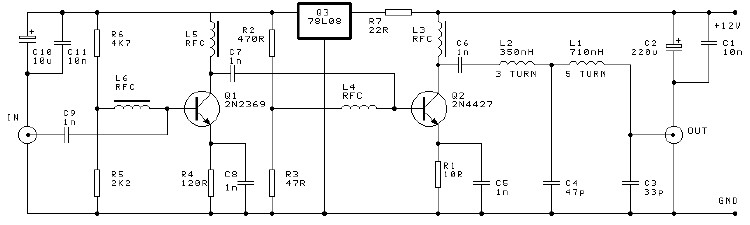
The circuit consists of two NPN transistors configured in a common-emitter arrangement, which is typical for VHF amplification applications. The initial transistor (Q1) receives the input signal, which is coupled through capacitor C9, allowing AC signals to pass while blocking any DC components. The amplified output from Q1 is then passed to Q2 through capacitor C7, further increasing the gain of the signal before it is delivered to the output stage.
Resistors R5 and R6 play critical roles in establishing the proper biasing conditions for Q1 and Q2, ensuring that both transistors operate in their active regions for optimal amplification. Inductor L6 is included in the biasing network to provide stability against variations in temperature and supply voltage, which can affect transistor performance.
The low-pass filter, designed to eliminate unwanted high-frequency signals, is essential for maintaining the purity of the output signal. This filter ensures that the amplified signal retains its quality, which is particularly important in VHF applications where spectral purity can significantly impact performance.
The inclusion of the 78L08 voltage regulator is a crucial design element, providing a stable voltage supply to the circuit. This regulator helps maintain consistent performance of the amplifier by compensating for fluctuations in the input supply voltage, thus ensuring that the output RF power remains stable and reliable even under varying operational conditions.
Overall, this VHF amplifier circuit is a robust solution for applications requiring high efficiency and reliable performance without the need for complex tuning or alignment procedures.A high efficiency simple 2-transistor VHF amplifier electronic circuit project can be designed using this electronic circuit diagram. This VHF amplifier electronic circuit has a very high efficiency of about 16dB gain, and requires no tuning or alignment procedures.
Wideband techniques have been used in the design and the circuit is equipped with a "lowpass" filter to ensure good output spectral purity. This VHF power amplifier circuit is specifically designed to amplify the output of 7mW to 10mW WBFM transmitters to a final level of 250mW to 300mW, after the filter. The transistor is biased by means of R5, R6 and L6, and the residual DC current is set by R4. The input signal is coupled by C9 to the Base of the transistor. The input signal from Q1 is coupled to the Base of Q2 via C7. The 78L08 voltage regulator is used to regulate the supply voltage to Q1 and the bias votages to both Q1 and Q2 so that the output RF power is relatively constant, even with large variations of supply voltage.
🔗 External reference
Related Circuits
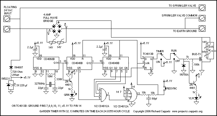
The resulting timer circuit is made from a CD4060, includes an oscillator and a 14 stage binary counter, two CD4040's, which are 12 stage binary counters, a CD4012 Dual Nand gate and a CD4013 Dual D Latch. The CD4060...
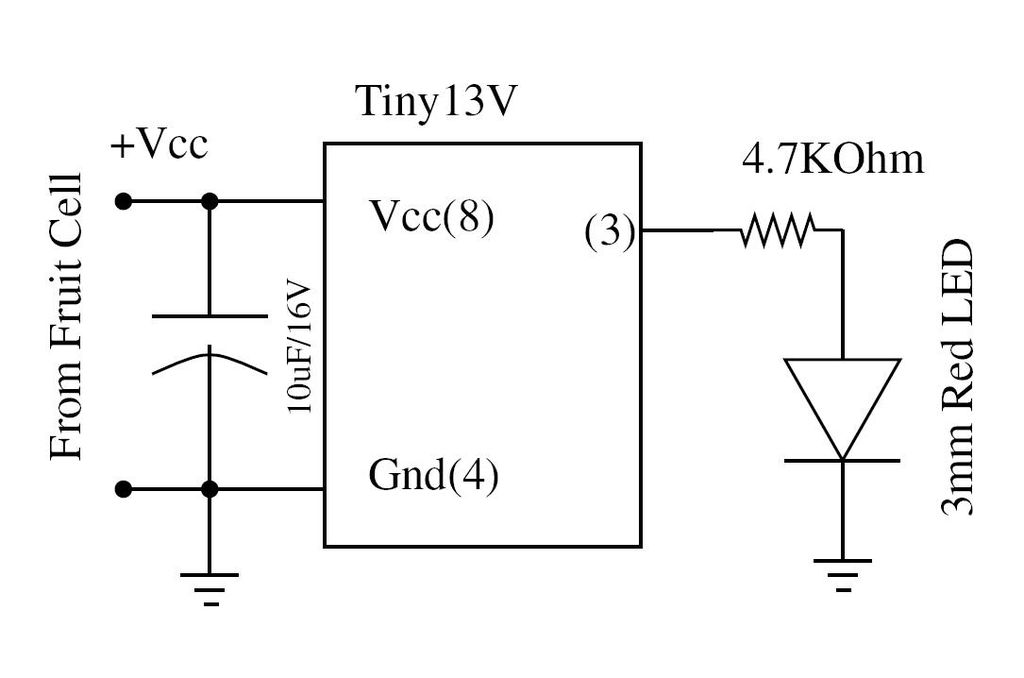
Wire the circuit diagram shown here on a breadboard. The choice of V type of AVR is important. For example, Tiny13V is very appropriate for such an application. To successfully implement the circuit diagram on a breadboard, several considerations must...
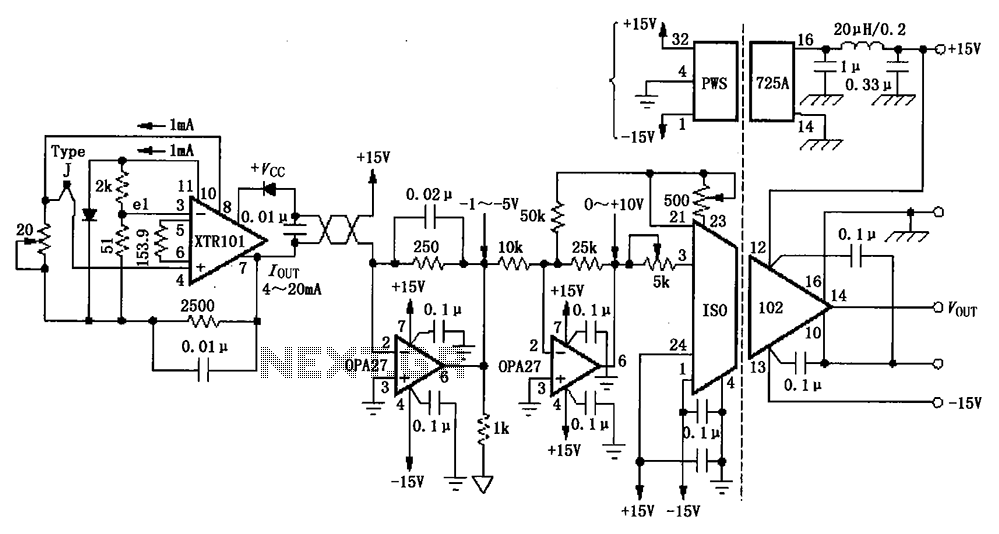
The circuit depicted in the figure features the ISO102 and XTR101 components, forming an isolated remote transmitter circuit equipped with isolated thermocouple cold-junction compensation. The circuit comprises four main parts: the current loop amplifier XTR101, the isolation amplifier ISO102,...

This design circuit is intended for sine wave oscillators, providing both sine and square wave outputs across a frequency range from below 20 Hz to above 20 KHz. The oscillation frequency can be easily adjusted by changing a single...
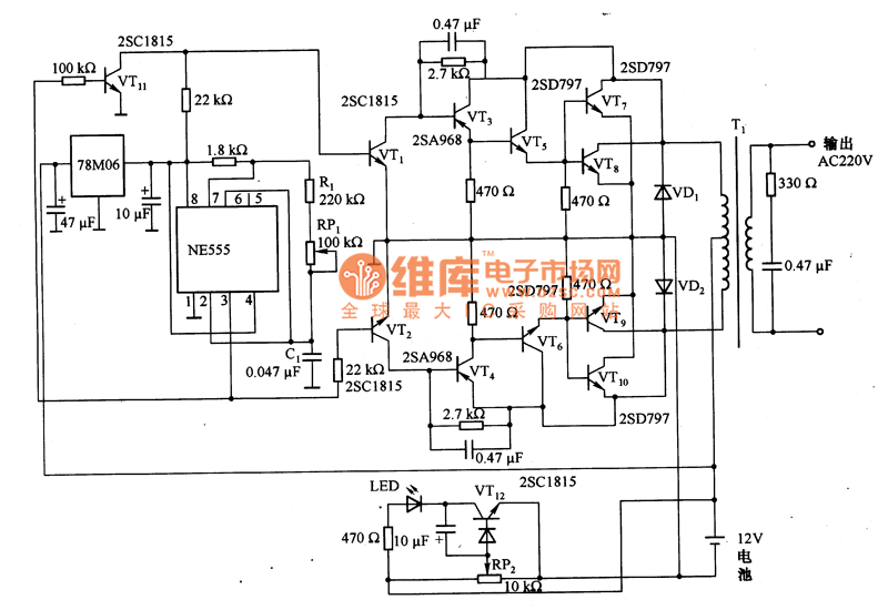
The inverter circuit diagram utilizing the NE555 timer is illustrated, designed to convert a +12V DC battery voltage into a 220V AC output voltage. In this circuit, the NE555 functions as an oscillator, with the oscillation frequency determined by...
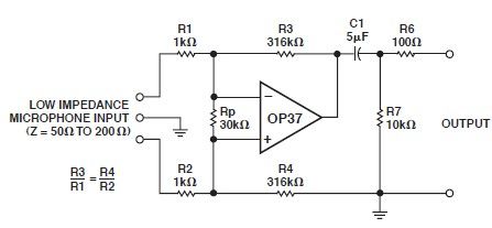
This microphone preamp schematic is an electronic circuit project utilizing the OP37 operational amplifier from Analog Devices. It functions as a fixed-gain transformerless microphone preamp, amplifying differential signals from low-impedance microphones by 50 dB, with an input impedance of...