
Schematic MP3 Car Audio Power AmplifierCircuits

The LF353 is pin compatible with the standard LM1558 allowing designers to immediately upgrade e the overall performance of existing LM1558 and LM358 designs. These amplifiers may be used in applications such as high speed integrators, fast D/A converters, sample and hold circuits and many other circuits requiring low input offset voltage, low input bias current, high input impedance, high slew rate and wide bandwidth.
The devices also exhibit low noise and offset voltage drift. (National Semiconductor) I recommended using IC NE5532. The NE5532 is a dual high-performance low noise operational amplifier. Compared to most of the standard operational amplifiers, such as the LM1458, LM1558, or LM4558 it shows better noise performance, improved output drive capability and considerably higher small-signal and power bandwidths. This makes the device especially suitable for application in high quality and professional audio equipment, instrumentation and control circuits, and telephone channel amplifiers.
The op amp is internally compensated for gains equal to one. If very low noise is of prime importance, it is recommended that the NE5532A version be used which has guaranteed noise voltage specifications. Features : Internally trimmed offset voltage: 10 mV Low input bias current: 50pA Low input noise voltage: 25 nV Low input noise current: 0.
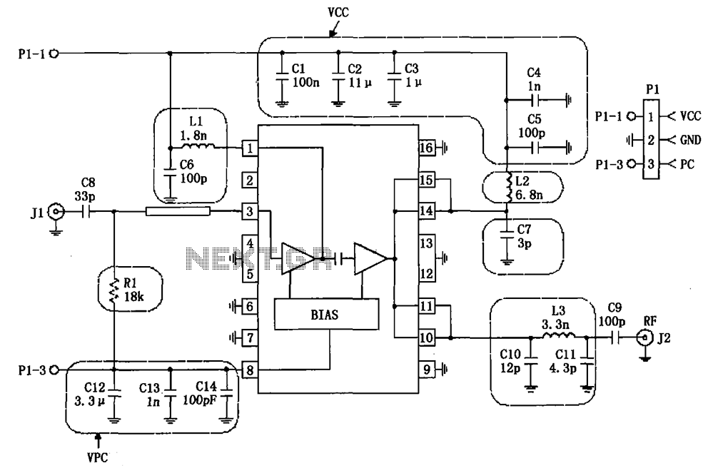
01 pA Wide gain bandwidth: 4 MHz High slew rate: 13 V/us Low supply current: 3. 6 m High input impedance: 1012. Low total harmonic distortion : When the Power amplifier is installed behind in the suitcase, we shall need a switch works stop. The LA47536 possesses a function stand by in it pin4. This pine require a small tension superior to 2V in start up the amplifier. Transistor Q1 and Q2 makes the function of walking stop for distance. When the driver activates the left indicator, either light the back fires or press on the brake, lamps rear ignite driving Q2 who he even made to drive Q1 who applies a tension > 2V on it pin4.
Overview - A pure complimentary structure that uses V-PNP transistors on the high side and NPN transistors on the low side to provide high power and superb audio quality. - The LA47536 includes almost all the functions required for car audio use, including a standby switch, a muting function, and each protection circuit.
It also provides a self-diagnosis function (output offset detection). (Sanyo) The pin 4 threshold voltage is set to be 2 VBE. When Vst is 2. 0V or higher, the amplifier will be on, and when Vst, is 0. 7V or lower, the amplifier will be off. Note that pin 4 requires an operating current of at least 40uA. The IC is set to the muted state by setting pin 22 to the ground potential. In this state, the audio output is muted. The time constant with which the muting function operates is set by an external RC circuit, and this time constant influences the pop noise that occurs when the amplifier is turned on or off. During steady state operation, the LA47536 detects, internally, whether or not an abnormal amplifier output offset has occurred, and outputs this signal from pin 25.
Applications can prevent speaker burnout and other problems by having the system microcontroller detect this pin 25 output signal and control either the standby state or the power supply. (An abnormal output offset may be caused by, for example, input capacitor leakage current. ) The pin 25 signal is turned off by setting pin 1 to the ground potential. In some cases, parasitic oscillations may be induced by the PCB layout. This oscillation can be eliminated by adding the components listed below. Note that the optimal capacitor value must be verified by testing in the actual mounted state in the end product.
Connect a capacitor and resistor (0. 1uF and 2. 2) in series between each output pin and ground. The frequency characteristics in the low frequencies can be improved by making the capacitance of the input capacitors variable. The recommended capacitance is 2. 2uF and smaller. Do not ground the outputs with the STBY voltage at around 1. 4V. Also, do not turn the IC off in the grounded state with a time constant provided for the STBY voltage.
Although the LA47536 includes an pop noise prevention circuit, pop noise can be reduced even further by using the muting function as well. Activate the muting function at the same time as power is applied. Then, after the output DC potential has stabilized, turn off the muting function. When turning the amplifier off, first turn on the muting function and then turn off the power supply.
These two methods are effective at minimizing pop noise. 🔗 External reference
Related Circuits
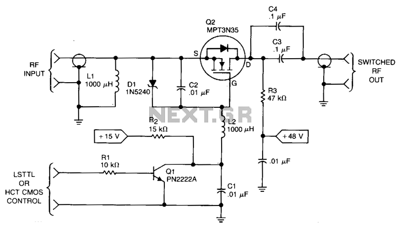
This RF power switch operates at 1.7 MHz with a 50-V source and load. Its on-loss is 0.2 dB, and its off-isolation is 30 dB. It provides 40-W PEP, 45 V_RMS, and 0.9 A_PEAK. The control input can come...
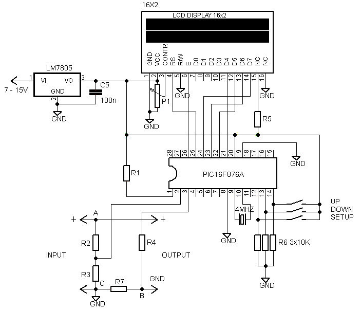
Voltmeters and ammeters with a PIC microcontroller can be utilized to measure voltage and current simultaneously. The configuration of voltmeters and ammeters using the PIC16F876A serves as a data processor for voltage and current measurements. This circuit employs a...
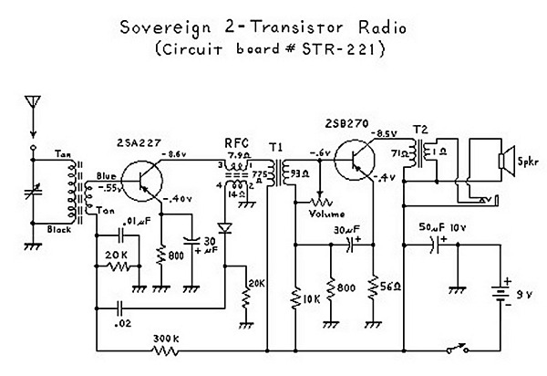
An analysis of certain radios reveals the impressive engineering by Japanese designers, particularly in creating a radio capable of driving a speaker with only two transistors. The first transistor (Q1) serves a dual function; it operates as an RF...
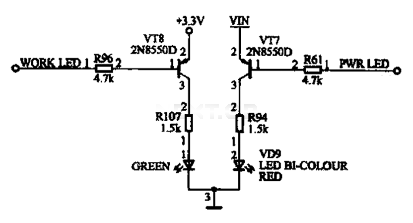
The ACER PM02 MP4 machine features a voltage status indicator circuit. When power is supplied, a red LED illuminates, indicating that the device is powered on. Upon entering operational mode, a green LED lights up. The voltage status indicator circuit...
The RF2132 linear power amplifier circuit is depicted in the provided figure. A radio frequency (RF) signal enters through input pin 3 and is processed via a preamplifier. The final stage of the amplifier outputs a gain of 10....
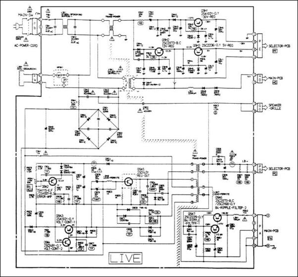
A 12V switching power supply schematic has been observed to generate significant heat, which has prompted discussions among users in prominent forums, such as dp. The 12V switching power supply is a crucial component in various electronic applications, providing...