
schematics Use of ground symbols in circuit diagrams

The TPS61200 is a synchronous step-up DC-DC converter designed for applications requiring efficient power management. The device features separate pins for GND and PGND to minimize noise interference in the circuit. The GND pin is intended for control and logic functions, while the PGND pin is dedicated to handling the power ground, which can carry higher currents and potentially induce noise if not properly managed.
In a typical application, the GND pin should be connected to a low-noise ground plane to ensure stable operation of the control circuitry. Conversely, the PGND pin should be connected to a separate ground plane that can handle the return currents from the power components without affecting the logic signals. This separation is crucial for maintaining the integrity of the feedback loop, which is essential for the regulation performance of the TPS61200.
The mention of chassis ground indicates a potential safety consideration, as connecting certain parts of the circuit to the chassis can provide a path for fault currents, enhancing the safety of the overall design. However, care must be taken to ensure that this connection does not introduce noise into the control circuitry. The recommendation to connect the bottom of R2 directly to the GND pin is a critical design consideration, as it helps to isolate the control signals from the noise generated by the power components, thus improving the overall performance and reliability of the power supply circuit.
In summary, the TPS61200's design necessitates careful attention to grounding practices to ensure optimal performance. The distinction between GND and PGND, as well as the consideration of chassis ground, plays a pivotal role in achieving a stable and efficient power management solution. Proper schematic representation and adherence to grounding principles are essential for the successful implementation of the TPS61200 in electronic designs.The TPS61200 spec says GND is control/logic ground and PGND is power ground but this isn`t reflected in the symbols chosen in the diagram. I`m also puzzled why the link to earth is shown on GND rather than on PGND. From this key it seems that various parts of the above circuit are to be tied to chassis ground and not to (say) digital/common/signal
/control/logic ground. Why specify chassis ground Am I wrong in interpreting that as the metal part of an enclosure which is (usually) tied to earth through the mains electrical connection for safety purposes. That symbol is not Building Earthing, it is circuit reference ground. That too need not be connected to building earthing, it`s just what any voltage in the circuit is referenced against.
Why they choose to connect to it I haven`t examined, I`ll look at the schematic later - that`s why I am not writing up an answer now. Anindo Ghosh May 2 `13 at 9:56 The bottom of R2 should connect directly to the GND pin on the TPS61200 to avoid power-ground noise upsetting the feedback and regulation of this device (and most other switching regulators should they have separate pins).
So, is this question just about the interpretation of symbols Andy aka May 2 `13 at 11:13 🔗 External reference
Related Circuits
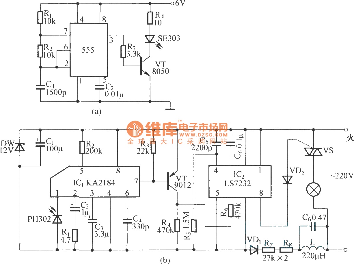
This is an infrared emission circuit diagram. The NE555 circuit generates a 40 kHz pulse, which is sent by the infrared emission control SE303 after being amplified by VT. The remote receiver and infrared dimming circuit are composed of...
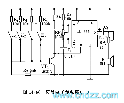
The controllable multivibrator, as illustrated in figure 14-40, consists of a 555 timer along with resistors RA, RP1, and capacitor C1. The oscillation frequency is influenced by the control voltage applied to pin 5. This control voltage is determined...
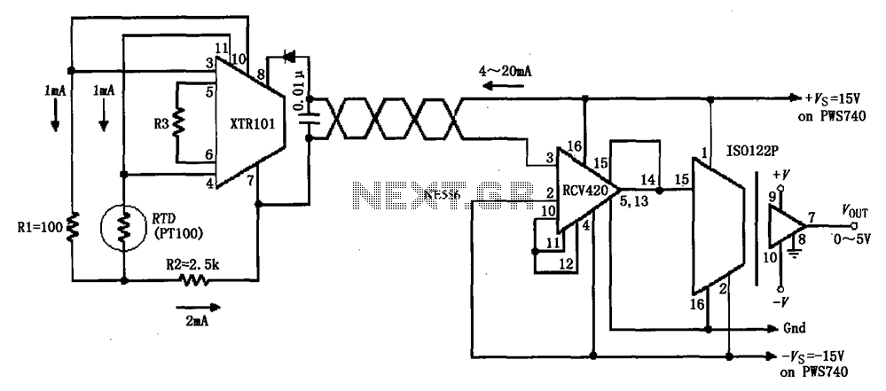
The circuit comprises an isolated RTD loop current configuration utilizing the XTR101 for transmitting loop current and the RCV420 for receiving it. The instrumentation amplifier detects changes in temperature via a resistance temperature detector (RTD), converting these changes into...
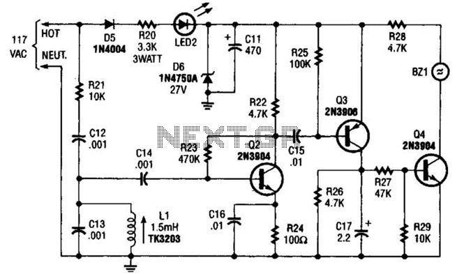
The baby-alert receiver consists of three transistors: Q2, configured as a high-gain linear amplifier; Q3, functioning as both an amplifier and detector; and Q4, which operates primarily as a switch. Additionally, there are several other components involved. The system...
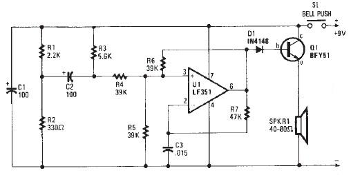
This electronic door buzzer circuit schematic has a straightforward function and is simple to construct. The circuit employs an LF351 operational amplifier along with a few common electronic components. When the S1 push-button is pressed, a positive voltage is...
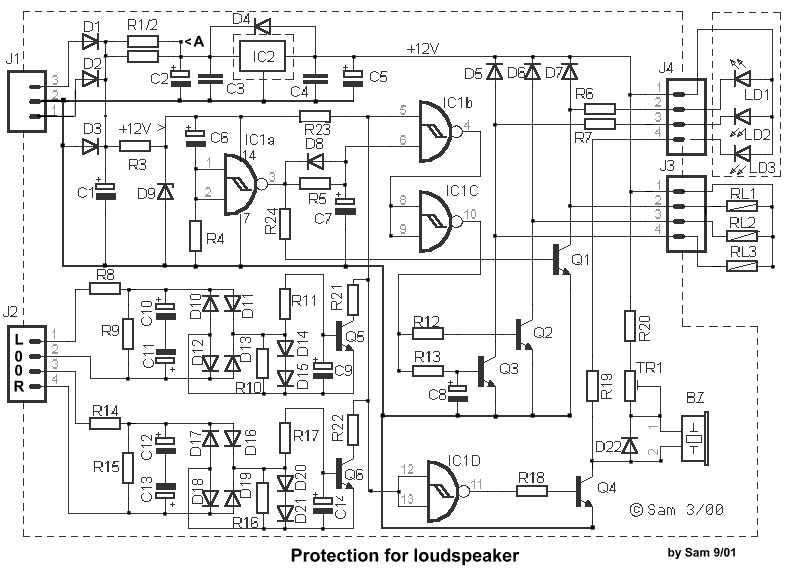
The circuit integrates several functions, including a smooth startup for the AC power line, with a one-second delay before connecting to the power supply transformers of the amplifier through relay RL1 and resistor Rx. This delay is designed to...