
Schmitt trigger zero crossing detector
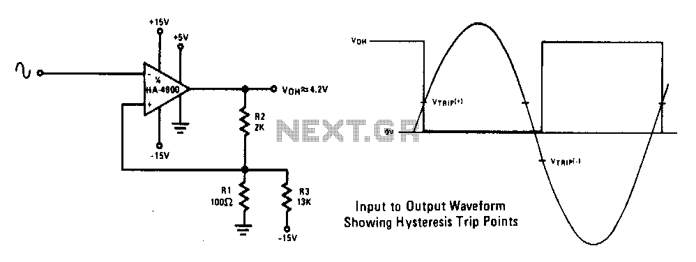
The circuit operates by utilizing hysteresis to create a threshold for signal transitions, effectively distinguishing between valid signals and noise. The 100 mV hysteresis ensures that once the input signal crosses a defined threshold, the output state changes, and it remains stable until the input signal drops below a second threshold. This characteristic is particularly beneficial in environments where input signals may be slow or prone to noise, allowing for reliable operation without unintended toggling of the output.
The waveforms associated with this circuit depict the input signal alongside the output response, clearly indicating the upper and lower trip points dictated by the hysteresis. When the input voltage exceeds the upper trip point, the output transitions to a high state. Conversely, when the input voltage falls below the lower trip point, the output returns to a low state. This clear demarcation between the trip points helps to prevent false triggering, ensuring that only significant changes in the input signal will affect the output.
The implementation of this circuit can be found in various applications, including signal conditioning, comparator circuits, and other digital logic systems where noise immunity and fast response times are critical. The design can be further enhanced by selecting appropriate components, such as operational amplifiers or dedicated comparator ICs, to optimize performance based on specific application requirements.This circuit has a 100 mV hysteresis which can be used in applications where very fast transition times are required at the output even though the signal is very slow. The hysteresis loop also reduces false triggering due to noise on the input The waveforms show the trip points developed by the hysteresis loop. 🔗 External reference
Related Circuits

These circuits are utilized for the detection of single-sideband (SSB) and continuous wave (CW) signals. The beat frequency oscillator (BFO) injection is generally in the range of 0.5 to 1 V rms for both circuits. The operational frequencies can...
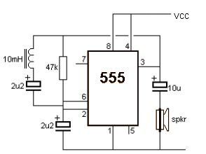
This metal detector electronic project schematic circuit is designed using a simple 555 timer integrated circuit. The schematic circuit requires few external electronic components. The metal detector circuit utilizes the 555 timer IC in an astable mode configuration, which generates...
A modification to David Knight's linear detector circuit was developed to create a high-fidelity AM receiver requiring an ultra-linear AM detector. The revised circuit eliminates the meter circuit and many bypass capacitors, resulting in a design with a finite...
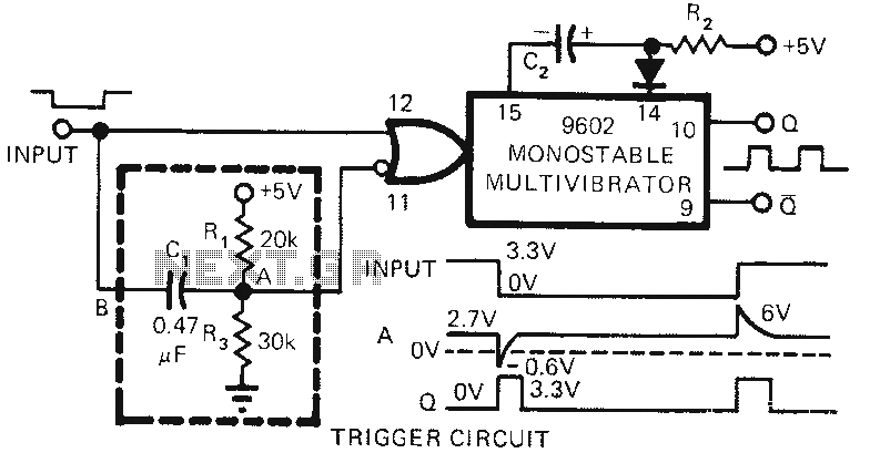
The 9602 multivibrator circuit can trigger either the rising edge or the falling edge of a square wave, but not both simultaneously. To enable double-edge triggering, two additional resistors and a capacitor can be employed. When the input signal...
The cooling is not only a PC using a small fan with an electronic commutator. A special feature of these fans is that their removal is less dependent on the load. Indicators monitoring the DC component of current may...

This is a simple RF bug detector designed to identify spy bugs, capable of operating up to 2 GHz. Below are some essential components required for this circuit. The RF bug detector circuit functions by utilizing radio frequency signals...