
SEQUENTIAL TIMER
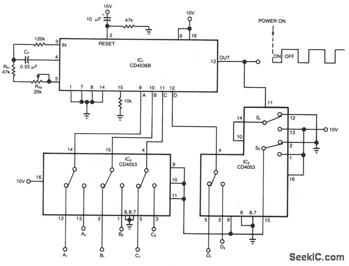
The timer circuit described is a versatile and robust design suitable for applications requiring precise timing control. The use of a CMOS programmable timer chip (IC1) allows for flexible configuration of timing intervals, which can be adjusted from milliseconds to minutes, accommodating a wide range of operational requirements. The internal structure of IC1, with its 24 ripple-binary counter stages, enables the generation of various timing sequences by bypassing the first eight stages as needed.
The oscillator circuit, comprising components CT, RT1, and RT2, is critical for establishing the timing frequency. Adjusting RT2 allows for fine-tuning the internal period (T1N), thus directly influencing the output timing intervals. The formula T_out = T1N * 2^(N-1) provides a straightforward means of calculating the output timing based on the selected counter stage, facilitating easy modifications to the timing characteristics.
The integration of CMOS triple SPDT analog switches (IC2 and IC3) enhances the circuit's functionality by allowing for the selection of different BCD codes for the on and off intervals. This feature enables the circuit to be controlled via manual toggle switches or programmable latches, offering flexibility in operation and ease of use. The design ensures that the output can be precisely controlled based on the desired timing sequence, making it suitable for various applications such as timers, alarms, and control systems.
To ensure reliable operation, the circuit incorporates measures to prevent race conditions during the switching process. The sequential operation of switches S1 and S2 in IC3 ensures that the circuit transitions smoothly between on and off intervals, while the parallel operation of the remaining switches allows for rapid changes without introducing timing errors.
Overall, this timer circuit exemplifies an efficient design that combines programmable timing capabilities with robust switching mechanisms, making it an ideal choice for applications requiring reliable and adjustable timing control.The timer circuit shown gives independent control of the output`s on and off intervals, which can range from 0. 055 seconds to 30 minutes, relatively unaffected by power-line transients. IC1 is a CMOS programmable-timer chip that includes 24 ripple-binary counter stages; the first eight are bypassed when logic 1 is applied to pin 6.
Then, a4-bit in put code at pins A, B, C, and D connects one of the 16 remaining stages to the output at pin 13. The chip includes an oscillator whose timing components are CT, RT1, and RT2. _For this example, you adjust RT2 for an internal period TlN of 54. 9 ms (18. 2 Hz). Then, the output on or off interval is: Tour= TIN2 N-1, where N is the number of counter stages in the internal divider chain (See Fig. 110-3). IC2 and IC3 are CMOS triple-spdt analog switches that connect one BCD code (A1 -D1) for the on interval and another (A2-D2) for the off interval.
You can apply the codes using manual toggle switches or programmable latches. When power is first applied, the switches are in the positions shown, which applies A1 -D1 to IC1 and generates the on intervat. When the output changes state, all the switches change position and initiate the off interval by applying, 42-D2 to IC1.
The cycle then repeats. To eliminate race conditions, switches S1 and S2 of IC3 operate in sequence before the remaining four switches operate in parallel. To start the output sequence with an off instead of an on interval, connect a power-on-set signal at pin 1 instead of the power-on-reset signal at pin 2.
🔗 External reference
Related Circuits
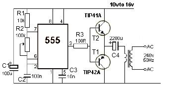
This 12V power inverter circuit can be utilized to power small devices that require 240 volts. It is particularly advantageous for operating 240-volt appliances using a 12-volt car battery. Unlike typical feedback oscillator inverters, this design employs a 555...
The goal is to create a timer activated by a button press, which will light three LEDs. After each 5-minute segment, one LED should turn off. After 15 minutes, a solenoid should ring a bell once. The individual has...
Do not use the on-board relay to switch mains voltage. The board's layout does not provide adequate isolation between the relay contacts and the low-voltage components. If mains voltage switching is required, mount a suitably rated relay in a...
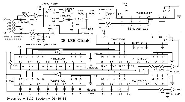
This is a programmable clock timer circuit that uses individual LEDs to indicate hours and minutes. 12 LEDs can be arranged in a circle to represent the 12 hours of a clock face and an additional 12 LEDs can...
The LTC6990 is a precision silicon oscillator with a programmable frequency range of 488Hz to 2MHz. It can function as either a fixed-frequency oscillator or a voltage-controlled oscillator (VCO). The LTC6990 belongs to the TimerBlox family of versatile silicon...
This circuit provides a visual 9-second delay using a 7-segment digital readout LED. When the switch is closed, the CD4010 up/down counter is preset to 9, and the 555 timer is disabled, holding the output high. When the switch...