
Shutter-speed tester
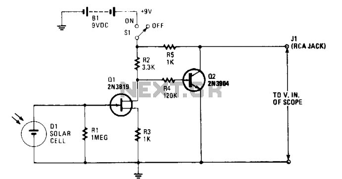
The described circuit operates based on the interaction between a solar cell and a pair of transistors, specifically a field-effect transistor (FET) and a bipolar junction transistor (BJT). The solar cell serves as a light sensor, converting incident light energy into electrical energy. When light strikes the solar cell, it generates a positive DC voltage, which is fed to the gate of the FET (Q1). This voltage effectively reduces the negative bias at the gate-source junction, which is initially established by a source resistor connected to the FET.
As the gate voltage increases, the drain current through the FET also increases due to the enhanced conductivity of the channel formed by the FET. The increase in drain current leads to a more negative voltage at the drain terminal of Q1. This change in voltage influences the operation of the second transistor, Q2, which is configured to respond to variations in the collector current of Q1.
The decrease in the drain voltage of Q1 results in a reduced base current flowing into Q2. Since the base current of Q2 is directly related to its collector current, a reduction in base current leads to a corresponding decrease in collector current. Consequently, the voltage at the collector of Q2 rises due to the reduced current flow, resulting in a more positive collector voltage.
The amplified output at the collector of Q2 is then directed to an oscilloscope's vertical input. This setup allows for real-time visualization of the voltage changes as a waveform on the oscilloscope display. The waveform reflects the intensity of light striking the solar cell; thus, any fluctuations in light levels will cause the waveform to shift vertically. This circuit effectively demonstrates the principles of light-to-voltage conversion and amplification, showcasing the interaction between photovoltaic elements and transistor-based amplification in electronic applications.The solar cell is connected across the input of the FET (field-effect transistor), Ql, so that it will produce positive dc voltage to the gate when activated by light shining through the open shutter, decreasing the negative gate-source bias already established by the source resistor, and causes an increase in drain current. The drain voltage goes more negative which causes a decrease in Q2's base current. Q2's collector current decreases, and its collector voltage becomes more positive. There is an amplified positive-going voltage output at the collector, and it's applied directly to the oscilloscope's vertical input, producing a waveform that is displaced vertically whenever light strikes the cell. 🔗 External reference
Related Circuits

This circuit is a simple device for testing the hfe (current gain) of both PNP and NPN transistors, with the capability to measure hfe values as high as 1000. It operates using two constant current sources formed by transistors...
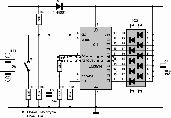
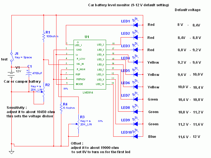
Car and Motorcycle Battery Tester Circuit. Going camping today often requires bringing various electronic devices for daily activities or entertainment. Typically, a charged lead-acid battery and a power source are essential. The Car and Motorcycle Battery Tester Circuit is designed...
This circuit is designed to prevent further damage to old equipment that may be in unknown condition, particularly to devices that are already shorted. The circuit functions as a protective measure for vintage or malfunctioning electronic devices. It is particularly...
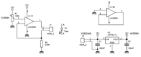
This led tester uses a power switched op-amp. The control range is about 0-30mA. Thus, all test and standard LEDs, the voltage across the LED to read. The power supply is an example lab power supply at least 15V,...
During rainy seasons, it can be quite bothersome when the car wipers operate continuously without pause. Have you ever considered implementing speed control for the wipers? While there are wiper control modules available commercially, many of them can be...

Before using LEDs, it is advisable to test them. An LED tester allows for testing even in low light conditions. LEDs are available in various shapes and colors, with some featuring clear, colorless packages and others having colored plastic...